Download

1 / 21
210 likes | 376 Views
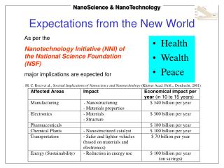
NanoScience & NanoTechnology. Expectations from the New World. As per the Nanotechnology Initiative (NNI) of the National Science Foundation (NSF) major implications are expected for. Health Wealth Peace.

E N D
NanoScience & NanoTechnology Expectations from the New World As per the Nanotechnology Initiative (NNI) of the National Science Foundation (NSF) major implications are expected for • Health • Wealth • Peace M. C. Roco et al., Societal Implications of Nanoscience and Nanotechnology (Kluwer Acad. Publ., Dordrecht, 2001).
NanoScience & NanoTechnology • Quantum Dot: Small clusters: ~103 - 106 atoms (bulk-like structure) but possess discrete excited electronic states if cluster diameter less than the bulk Bohr radius, ao, (typically < 10 nm) Bottom-up Approach To synthesize material from atoms or molecules by means of “self-assembly”. Spectroscopic Regions: • Molecule: Ultra-small clusters: 10 – 100 atoms show strongly deviating molecular structures from the bulk. E.g.: Si13 (metallic-like close packing) Si45 (distorted diamond lattice) Si13 Si45 U. Rothlisberger, et al., Phys. Rev. Lett. 72, 665 (1994).
NanoScience & NanoTechnology Cont. Spectroscopic Regions: • Polariton: Large “clusters”: > 106 atoms. In this regime the particle acts as an optical cavity (micro-cavity) due to light matter coupling -> Polariton Laser Kinetic Regions: Consideration of the transport properties in the media. In semiconductors one experiences in nanocrystals: < 106 atoms: Molecular decay kinetics > 106 atoms: Many body kinetics (Auger recombinations etc. ) -> important in Si nanocrystal luminescence
NanoScience & NanoTechnology Quantum Confinement
NanoScience & NanoTechnology Quantum Devices and Quantum Effects 200 200 nm2 SFM image of InAs dots on GaAs R. Notzel, Semicond. Sci. Techn. 11, 1365 (1996). White and blue emitting solid-state devices based on quantum dotsdeveloped in Sandia National Laboratories. Sandia National Laboratories, (2003).
NanoScience & NanoTechnology Molecular Devices / Gates Current-Voltage Characteristics Use of nanotubes in Field-Effect Transistors (FET) IBM: Applied Physics Letters, vol 73, p. 2447 (1998) at room temperature (290 K) acts like a FET at 77K: acts like a single electron transistor (SET)
NanoScience & NanoTechnology Top-down Approach To create and investigate the Nanoscale by means, for instance, of lithographical methods and high sensitive measurements. In gates with 2 nm width it has been shown that the channel conductance is quantized in steps of 2e2/h. 100 nm MOSFET (gm=570 mS/mm, fT=110 GHz). D. M. Tennant, in Nanotechnology, edited by G. Timp (AIP Press, Springer Verlag, New York, 1999), p. 161.
NanoScience & NanoTechnology Nanofabrication and Lithography Emission of atomic hydrogen (Lyman-a line) Nearfield Exposure (not wavelength limited) Photolithographic contact printing with phase shifting mask. V. Liberman, M. Rothschild, P. G. Murphy, et al., J. Vac. Sci. Techn. B 20, 2567 (2002).
NanoScience & NanoTechnology Lithographical Techniques • Photo emission • X-rays • Electrons • Ions • SPM (not sketched, see below)
NanoScience & NanoTechnology Dip-Pen Nanolithography Submicrometerarrays of biomolecules as screening tools in proteomics and genomics. Ki-Bum Lee, JACS 2003, 125, 5588
NanoScience & NanoTechnology Lithographical Techniques Challenges be met by current laboratory methods before they can be seriously considered Optical step and repeat reduction printing SPM D. M. Tennant, in Nanotechnology, edited by G. Timp (AIP Press, Springer Verlag, New York, 1999), p. 161. for 50 % coverage (e.g., equal lines and spaces)
NanoScience & NanoTechnology Nanoscale Imaging SFM Study STM Study Self-assembly of C18ISA on HOPG surface Lipid Bilayer (LB Technique) on silicon oxide surface R.M. Overney, Phys. Rev. Lett. 72, 3546-3549 (1994) S. De Feyter et al. in Organic Mesoscopic Chemistry, Ed. H. Masuhara et al., Blackwell Science 1999
NanoScience & NanoTechnology e.g. Film Thickness Limitation for the Photoresist in Photo-Lithography The absorption coefficient imposes a max. thickness on the photoresist T. M. Bloomstein, M. Rothschild, R. R. Kunz, et al., J. Vac. Sci. Techn. B 16, 3154 (1998). Constraints in the New World The Nanoscale is not only about small particles or small patterns but also about material limitation.
NanoScience & NanoTechnology However, the reality of photolithographical imperfections (see below) suggests PAG distribution inhomogeneities. SUBSTRATE Fat Bottoms T - tops Other constraints for the Photoresist Ideally: A photoresist consists of a Polymer Matrix (e.g., PMMA) consisting of acid-labile groups and “homogeneously” distributed photoacid generators (PAG). Photoresist with “Homogeneous” PAG distribution
NanoScience & NanoTechnology Spincoated Ultrathin Films In polymeric systems, the molecular mobility is of particular concern if length scales below ~ 100 nm are involved Illustrated with a study on:
NanoScience & NanoTechnology Scan Size 50 50 mm2 tPEP 400 nm Scan Size 10 10 mm2 tPEP 4 nm Spin Coating Effect on Polymer Mobility below the 100 nm Film Thickness Regime R.M. Overney et al., J. Vac. Sci. Techn. B 14(2), 1276-1279 (1996).
Dewetting and Spincoated Ultrathin Films NanoScience & NanoTechnology 1.0 0.8 0.6 0.4 0.2 0.0 Normalized Lateral Force 0 100 200 300 400 Dewetting hole velocities as function of the PEP film thickness Dewetting Velocity (▲ Poly(vinyl pyridine (PVP) screener to silicon substrate) Lateral Force PEP Si Lateral Force and dewetting kinetics suggest the formation of a rheologically modified boundary layer of PEP towards the silicon substrate → “glassification” of PEP R.M. Overney et al., J. Vac. Sci. Techn. B 14(2), 1276-1279 (1996).
Confined Boundary Layer of Spincoated Ultrathin Films NanoScience & NanoTechnology BULK Mean field theories consider the effect of pinning at interfaces only within a pinning regime (0.6 – 1 nm « Rg) ~ 100 nm SRZ BULK ICZ ~ 1 nm ICZ S S Lateral Force and Dewetting Studies suggest that the PEP phase is rheological modified within a 100 nm boundary region that exceeds by two orders of magnitude the theoretically predicted pinning regime of annealed elastomers at interfaces with negative spreading coefficient.
Entanglement Strength and Spincoated Ultrathin Films NanoScience & NanoTechnology Entanglement strength studies on poly (ethylene-propylene) (PEP) films revealed interfacial confinement effects on the transition load from 3D viscous shear to 2D chain sliding. t = 520 nm Transition Point Pt • Entanglement Strength (a) low load sliding regime (b) high friction coefficient 1 = 2.1 3D flow (c) low friction coefficient 2 = 0.3 2D sliding C. K. Buenviaje, S. Ge, M. Rafailovich, J. Sokolov, J. M. Drake, R. M. Overney, Confined Flow in Polymer Films at Interfaces, Langmuir, 19, 6446-6450, (1999). • No transition, only 2D chain sliding is observed on films < ~ 20 nm thick (ICZ). • Transition load increases with thickness up to ~230nm (SRZ). • Transition load is constant for films thicker than ~230 nm (BULK).
Interfacially Confined Spincoated Ultrathin Films NanoScience & NanoTechnology Structural Model • At a thickness of 20 nm the polymer films are in a gel-like state (“porous structure”). [ X-ray reflection data of L.W. Wu] Chains are fully disentangled due to high shear stresses. • The polymers adjacent to the sublayer diffuse into the porous structure of the sublayer. [Neutron Reflectivity studies on polystyrene, X. Zheng et al. Phys. Rev. Lett. 74, 407 (1995)] two-fluid system • The anisotropy generated in normal direction recovers slowly over a distance of about 7-10 Rg. • Temperature annealing causes the gel to shrink and to “freeze” the anisotropic boundary structure. [Neutron Reflectivity studies on polystyrene, X. Zheng et al. Phys. Rev. Lett. 74, 407 (1995)]
NanoScience & NanoTechnology Material Property Engineering Engineering with Molecular Weight Engineering with Crosslinking