Download
1 / 1
10 likes | 100 Views
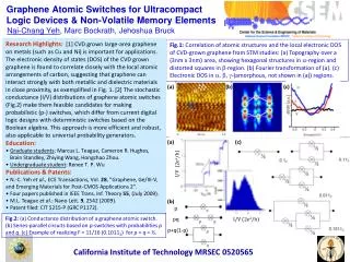
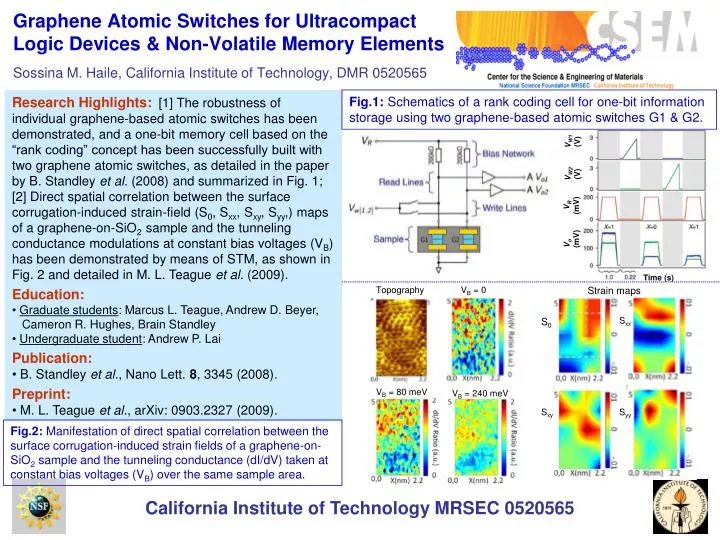
V W1 (V). V W2 (V). V R (mV). V o (mV). Topography. V B = 0. V B = 80 meV. V B = 240 meV. Graphene Atomic Switches for Ultracompact Logic Devices & Non-Volatile Memory Elements Sossina M. Haile, California Institute of Technology, DMR 0520565.

E N D
VW1 (V) VW2 (V) VR (mV) Vo (mV) Topography VB = 0 VB = 80 meV VB = 240 meV Graphene Atomic Switches for Ultracompact Logic Devices & Non-Volatile Memory ElementsSossina M. Haile, California Institute of Technology, DMR 0520565 • Research Highlights:[1] The robustness of individual graphene-based atomic switches has been demonstrated, and a one-bit memory cell based on the “rank coding” concept has been successfully built with two graphene atomic switches, as detailed in the paper by B. Standley et al. (2008) and summarized in Fig. 1; [2] Direct spatial correlation between the surface corrugation-induced strain-field (S0, Sxx, Sxy, Syy,) maps of a graphene-on-SiO2 sample and the tunneling conductance modulations at constant bias voltages (VB) has been demonstrated by means of STM, as shown in Fig. 2 and detailed in M. L. Teague et al. (2009). • Education: • Graduate students: Marcus L. Teague, Andrew D. Beyer, • Cameron R. Hughes, Brain Standley • Undergraduate student: Andrew P. Lai • Publication: • B. Standley et al., Nano Lett. 8, 3345 (2008). • Preprint: • M. L. Teague et al., arXiv: 0903.2327 (2009). Fig.1: Schematics of a rank coding cell for one-bit information storage using two graphene-based atomic switches G1 & G2. Time (s) Strain maps Sxx S0 Sxy Syy Fig.2: Manifestation of direct spatial correlation between the surface corrugation-induced strain fields of a graphene-on-SiO2 sample and the tunneling conductance (dI/dV) taken at constant bias voltages (VB) over the same sample area. California Institute of Technology MRSEC 0520565