Download

1 / 20
200 likes | 350 Views
Lab Environment and Miniproject Assignment. Fall 2008 ECE554 Digital Engineering Laboratory. Lab Environment. Ten 1.8 GHz Core 2 Duo Workstations with 4 GB RAM and 200GB Harddrives Design Tools Xilinx ISE – Integrated Software Environment Xilinx EDK – System Level Integration Software

E N D
Lab Environment and Miniproject Assignment Fall 2008 ECE554 Digital Engineering Laboratory
Lab Environment • Ten 1.8 GHz Core 2 Duo Workstations with 4 GB RAM and 200GB Harddrives • Design Tools • Xilinx ISE – Integrated Software Environment • Xilinx EDK – System Level Integration Software • Modelsim – Simulation Environment • Instrumentation • Hewlett-Packard Oscilloscopes – probing logic values • Agilent Logic Analyzers – monitor data on output pins • Xilinx Virtex2-Pro FPGA Boards
Lab Warnings • Do not wear static electricity generating clothing (wool sweaters) • Report stuff dripping from ceiling (don’t touch it). • Don’t sit or stand on backs of chairs or lab tables • Don’t probe (with oscilloscope) or touch anything on the FPGA board, except for push buttons, DIP switches, and special pins for clocks and expansion headers (left and right sides of board) • Do not do any wiring on the board with power on • Be sure you download the correct files to the FPGA • Carefully read all warnings in Lab Environment handout
Virtex2-Pro Board: Features • Xilinx Virtex FPGA (Compute) • 256 MB DDR Memory (PC2100) (Store for Read/Write) • Serial Ports to PC (I/O from/to Outside World) • Keyboard/Mouse (PS/2) Port • VGA Output to VGA Monitor • Audio/Video Converters • See Virtex2-Pro Board Manual at: http://www.digilentinc.com/Data/Products/XUPV2P/XUPV2P_User_Guide.pdf
Current Setup USB Cable Serial Cable Virtex2-Pro Board machine running HyperTerminal USB port: Configuration download Serial port: Miniproject
Miniproject Specification • For the miniproject, you will • Design a Special Purpose Asynchronous Receiver/Transmitter (SPART) and its testbench in Verilog/VHDL • Simulate the design to ensure correct performance • Download the design and associated files and demonstrate correction functionality • Prepare a report on your design
Miniproject Objectives • To get familiar with the lab environment prior to the class project and bench exam • To get practice using HDL in your designs • To provide the basic I/O interface to the class project • To get experience working with a partner
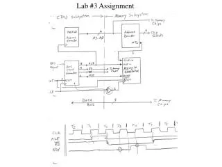
Processor Interface • Data is sent/received across the “bidirectional” data bus • Handshaking (status) signals • TBR: Transmit Buffer Ready (Empty) • RDA: Receive Data Available • IOCS: Chip Select • IOR/W_: Read or Write Bar signal
Asynch. Serial Communication • Start bit (1 bit wide) • Data bits (8 bits) • Parity(None, Even, Odd) - optional • Stop bit (1 bit wide)
Transmitting • Tx must be tested first. • Tx shifts the “LSB” out from Tx buffer first. • Tx sends “stop bit” when there is nothing to send.
Receiving • Receiver samples the RxD to get the beginning of the “start bit” • Use “resynchronization” to avoid “metastability” of any flip-flop
Baudrate and Sampling • We want the transmission rate to be constant for different input clocks • Baud rates of 4800 and 9600 bit per second • Sampling rate = x16 of the baud rate (bit rate) • Divide the clock to get the “Enable” signal (sampling rate)
Testbench • Previously a mock processor implemented as a simiple finite state machine • Use the EDK to interface your SPART to a bus which can communicate with a PowerPC processor • Receive data on the RxD from keyboard and transmit (echos) back on the TxD back to the HyperTerminal • Implement a simplified printf that can print character strings • Load Baud Rate Generator with Arbitrary value • Demonstrate ability to work at different Baud Rates using the BRG register
Demonstration Show the ability to receive and transmit characters at 4800 and 9600 buad rates. • Demos to be done in lab on 9/18 at start of class.
Miniproject Report • Due 9/18 at start of class • Verilog/VHDL code for your design with clear comments • Description of the function of the SPART and each block in the design, including the testbench • Record of experiments conducted and how the design was tested • Problems encountered and solutions employed