Download
1 / 90
900 likes | 1.05k Views
Tutorial3: NEMO5 Models. Jean Michel D. Sellier , Tillmann Kubis, Michael Povolotskyi , Jim Fonseca, Gerhard Klimeck Network for Computational Nanotechnology (NCN) Electrical and Computer Engineering. A short introduction. A short introduction…. A short introduction.

E N D
Tutorial3: NEMO5 Models Jean Michel D. Sellier, Tillmann Kubis, Michael Povolotskyi, Jim Fonseca, Gerhard Klimeck Network for Computational Nanotechnology (NCN) Electrical and Computer Engineering
A short introduction A short introduction…
A short introduction 18 years development • Texas Instruments • NASA JPL • Purdue • Peta-scale Engineering • Gordon Bell • Science, Nature Nano
…in this tutorial …in this tutorial
…in this tutorial • Why should one use a atomistic approach today? • Why should one use a atomistic approach today? • What are the models implemented? • How to prototype a new solver? • Example of simulations • Exercises
…in this tutorial • Why should one use a atomistic approach today? • What are the models implemented? • Why should one use a atomistic approach today? • What are the models implemented? • How to prototype a new solver? • Example of simulations • Exercises
…in this tutorial • Why should one use a atomistic approach today? • What are the models implemented? • How to prototype a new solver? • Why should one use a atomistic approach today? • What are the models implemented? • How to prototype a new solver? • Example of simulations • Exercises
…in this tutorial • Why should one use a atomistic approach today? • What are the models implemented? • How to prototype a new solver? • Example of simulations • Why should one use a atomistic approach today? • What are the models implemented? • How to prototype a new solver? • Example of simulations • Exercises
…in this tutorial • Why should one use a atomistic approach today? • What are the models implemented? • How to prototype a new solver? • Example of simulations • Exercises • Why should one use a atomistic approach today? • What are the models implemented? • How to prototype a new solver? • Example of simulations • Exercises
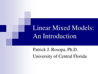
Why an atomistic approach? • The miniaturization of devices has reached the point where thenumber of atoms is countable. Simulation and STM image of a Silicon wire, only 1 atom tall, 4 atoms wide!! [1] B. Weber, et al. “Ohm’s Law Survives to the Atomic Scale”, Science 6 January 2012, Vol. 335 no. 6064 pp. 64-67 DOI: 10.1126/science.1214319 [2] http://physicsforme.wordpress.com/2012/01/07/ohms-law-survives-to-the-atomic-scale/
Why an atomistic approach? • The miniaturization of devices has reached the point wheregeometries are in 3 dimensions. [3] www.intel.com
Multi-scale and Multi-Physics approaches Multi-Scale approach
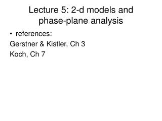
Multi-scale and Multi-Physics approaches • Many modern devices can be considered as constituted of a fully quantum active (small) area and a fully semi-classical (big) area. [10] http://purdue.academia.edu/GerhardKlimeck/Papers/1238240/Quantum_and_semi-classical_transport_in_NEMO_1-D • Many modern devices can be considered as constituted of a fully quantum active (small) area and a fully semi-classical (big) area.
Multi-scale and Multi-Physics approaches Multi-Physics approach
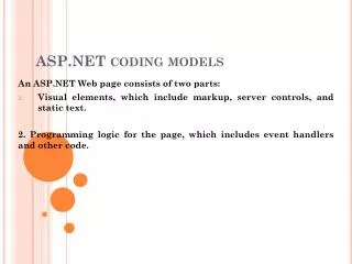
Multi-scale and Multi-Physics approaches • Several modern device need a multi-physics approach. [13] M. Usman et al., “Moving Toward Nano-TCAD Through Multimillion-Atom Quantum-Dot Simulations Matching Experimental Data”, IEEE Transactions on Nanotechnology, Vol. 8, No. 3, May 2009.
Multi-scale and Multi-Physics approaches • Long range calculationsStrain experienced by an InAs dot inside a GaAs structure. • Short range calculationsWavefunctions inside a InAs dot or in a small area surrounding the InAs dot. • Strain experienced by an InAs dot inside a GaAs structure. • Wavefunctions inside a InAs dot or in a small area surrounding the InAs dot.
What are the models implemented in NEMO5? What are the models implemented in NEMO5?
What are the models implemented in NEMO5? Note: • NEMO5 can be seen as a general framework so it can virtually contain any number of model (solver). • The real question to ask is:What are the model implemented so far.. Note: • NEMO5 can be seen as a general framework so it can virtually contain any number of model (solver). • The real question to ask is:What are the model implemented so far..
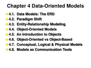
What are the models implemented in NEMO5? D1 InAs D2 GaAs AlSb InP D3 Si Ge Materials definition Domain definition Simulation Domains consist of regions Every region has a material Domains go to solvers Solvers interaction Definition of solver input/output
What are the models implemented in NEMO5? • The models/methods so far implemented in NEMO5 are divided in categories:Strain modelsPhononsTight Binding methodElectronic StructureTransport • The models/methods so far implemented in NEMO5 are divided in categories:
What are the models implemented in NEMO5? • The models/methods so far implemented in NEMO5 are divided in categories:Strain modelsPhononsTight Binding methodElectronic StructureTransport • The models/methods so far implemented in NEMO5 are divided in categories:Strain models
What are the models implemented in NEMO5? • The models/methods so far implemented in NEMO5 are divided in categories:Strain modelsPhononsTight Binding methodElectronic StructureTransport • The models/methods so far implemented in NEMO5 are divided in categories:Strain modelsPhonons
What are the models implemented in NEMO5? • The models/methods so far implemented in NEMO5 are divided in categories:Strain modelsPhononsTight Binding methodElectronic StructureTransport • The models/methods so far implemented in NEMO5 are divided in categories:Strain modelsPhononsElectronic Structure
What are the models implemented in NEMO5? • The models/methods so far implemented in NEMO5 are divided in categories:Strain modelsPhononsTight Binding methodElectronic StructureTransport • The models/methods so far implemented in NEMO5 are divided in categories:Strain modelsPhononsElectronic StructureTransport
What are the models implemented in NEMO5? Strain Models
Strain Models • What is a strain?A crystal experiences strain when it undergoes some stress which raises its internal energy in comparison to its strain-free reference compound.
Strain Models • What is a strain?A crystal experiences strain when it undergoes some stress which raises its internal energy in comparison to its strain-free reference compound. • When does a crystal experience it?Nanostructures composed of materials with different lattice constants always exhibit strain.
Stranski-KrastanowGrowth Strain Models Self-Assembly Process InAs deposition on GaAs substrate InAs (0.60583 nm) First Layer (wetting layer) ~ 1ML GaAs (0.56532 nm) GaAs InAs InAs GaAs GaAs
Strain Models Valence Force Field Harmonic Anharmonic Keating Several flavors
Strain Models • The strain calculations is an optimization problem.Strategy:We calculate the total energy of the crystal and find the atoms position that minimize the total energy.Method:The minimization is done by means of a Newton optimization method that is based on the calculation of the Jacobian and the Hessian of the total elastic energy. • Strategy:We calculate the total energy of the crystal and find the atoms position that minimize the total energy.
Strain Models • The strain calculations is an optimization problem.Strategy:We calculate the total energy of the crystal and find the atoms position that minimize the total energy.Method:The minimization is done by means of a Newton optimization method that is based on the calculation of the Jacobian and the Hessian of the total elastic energy. • Strategy:We calculate the total energy of the crystal and find the atoms position that minimize the total energy.Method:The minimization is done by means of a Newton optimization method that is based on the calculation of the Jacobian and the Hessian of the total elastic energy.
Strain Solver Options • models • linear_solver • preconditioner
Strain Solver Options • max_num_iters • absolute_tol • relative_tol
Strain Solver Options • More options in the manual…
Electronic Structure Electronic Structure
Electronic Structure • Electronic structure of a device can be studied by means of Schroedinger-Poisson systems in tight-binding formalism.The Schroedinger equation is rewritten using the tight-binding method.The Schroedinger equation is solved on a atomistic meshThe Poisson equation is solved on a Finite Element Mesh (FEM). • Electronic structure of a device can be studied by means of Schroedinger-Poisson systems in tight-binding formalism.
Electronic Structure • Electronic structure of a device can be studied by means of Schroedinger-Poisson systems in tight-binding formalism.The Schroedinger equation is rewritten using the tight-binding method.The Schroedinger equation is solved on a atomistic meshThe Poisson equation is solved on a Finite Element Mesh (FEM). • Electronic structure of a device can be studied by means of Schroedinger-Poisson systems in tight-binding formalism.Schroedinger equation - tight-binding.Poisson equation - Finite Element Mesh (FEM).
Tight-Binding Method • The underlying ideas of the tight-binding approach are:electrons are considered to be tight binded to the potential core.selection of a basis consisting of atomic orbitals (such as s, p, d, f, and s*) centered on each atom. • [12] http://thisquantumworld.com/wp/the-technique-of-quantum-mechanics/the-hydrogen-atom/
A few words on passivation In-plane quantum well bandstructure Bare surfaces Passivated surfaces Bulk band gap Bulk band gap Result: Surface states successfully shifted to high energies
Poisson Solver Options • atomistic_output
Poisson Solver Options • node_potential_output
Poisson Solver Options • one_dim_output