Download
1 / 1
10 likes | 132 Views
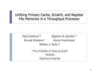
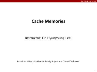
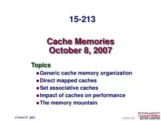
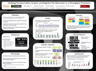
Unifying Primary Cache, Scratch, and Register File Memories in a Throughput Processor. Traditional Design. Proposed Unified Design. Streaming Processor (SM). Program A Program B. Register File. Register File Hierarchy.

E N D
Unifying Primary Cache, Scratch, and Register File Memories in a Throughput Processor Traditional Design Proposed Unified Design Streaming Processor (SM) Program A Program B Register File Register File Hierarchy Mark Gebhart1,2 Stephen W. Keckler1,2 Brucek Khailany2 Ronny Krashinsky2William J. Dally2,3 1The University of Texas at Austin 2NVIDIA 3Stanford University Register File Register File Shared Memory Main Register File Shared Memory Cache MRF (4 banks) MRF (4 banks) MRF (4 banks) Unified (4 banks) Unified (4 banks) Unified (4 banks) Shared Memory Cache Shared Memory Cache MEM Unit MEM Unit MEM Unit MEM Unit MEM Unit MEM Unit Cache SIMT Lanes ALU SFU MEM TEX Cache Tags Shared Memory / Cache Crossbar Cache Tags Shared Memory / Cache Crossbar Shared Memory (32 banks) Cache (32 banks) Motivation Overview • GPUs have thousands of on-chip resident threads • On-chip storage per thread is very limited • On-chip storage split between register file, scratchpad, and cache • Applications have diverse requirements between these three types of on-chip storage • Efficiently utilizing on-chip storage can improve both performance and energy Results • Performance and energy overheads for benchmarks that do not benefit are less than 1% • Performance improvements up to 71% along with significant energy and DRAM reductions • Automated algorithm determines most efficient allocation • Overheads are mitigated by leveraging prior work on register file hierarchy Background Microarchitecture • 32 SMs per chip • Each SM contains: • 32 SIMT lanes • Register file hierarchy • 256KB main register file • 64KB shared memory • 64KB primary data cache • Total of 96 banksin baseline design • Unified design has only 32 banks • Challenges: • Bank access energy • Bank conflicts Baseline Allocation Algorithm Unified • Allocate enough registers to eliminate spills • Programmer dictates shared memory blocking • Maximize thread count subject to register and shared requirements • Devote remaining storage to cache Methodology Related Work • Fermihas a limited form of flexibility between shared memory and cache, programmer chooses either: • 16KB shared memory and 48KB cache • 48KB shared memory and 16KB cache • Generated execution and address traces with Ocelot • Performance and energy estimates come from custom SM trace-based simulator • 30 CUDA benchmarks drawn from CUDA SDK, Parboil, Rodinia, GPGPU-sim • 22 with limited memory requirements that don’t benefit • 8 that see significant benefits