Download
1 / 16
160 likes | 311 Views
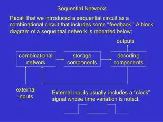
Sequential Networks Recall that we introduced a sequential circuit as a combinational circuit that includes some “feedback.” A block diagram of a sequential network is repeated below:. outputs. combinational network. storage components. decoding components. external inputs.

E N D
Sequential Networks Recall that we introduced a sequential circuit as a combinational circuit that includes some “feedback.” A block diagram of a sequential network is repeated below: outputs combinational network storage components decoding components external inputs External inputs usually includes a “clock” signal whose time variation is noted.
To design a sequential network, we need to specify: • the combinational network • the storage components • the decoding elements • The design process proceeds as follows: • A problem statement needs to be converted into a State Diagram. (This specifies the nature of the storage components.) • From the State Diagram, obtain a State Table. • Derive the FF (storage elements) input equations from the “next-state” entries in the State Table. (This resolves the combinational network.) • Derive output equations from the output entries in the State Table. (This specifies the decoding elements.) • (All of these terms will become clearer as we proceed.)
An example: We want to design a sequential circuit that recognizes a particular sequence of bits. Such a circuit could be useful in many applications where two areas are: • codes for unlocking a door (or access to another secure entitiy) • determining if a message (on a communication channel such as the “Internet”) is intended for a particular link on the channel. Sequence detector X Z We need to be able to “start” the sequence detector from a known, given, state.
The requirements of our circuit are to include the following (for this case only): • We want to recognize when X = 1101 (earliest to latest) no matter where that sequence of bits occurs in the message stream. An example of what might happen: • X = 0 0 1 0 1 1 0 1 1 0 … • At the point at which this happens we set Z = 1, otherwise Z = 0. (After we have detected “110” in the past and a “1” occurs, we set Z = 1). • We develop a logical sequence of states that reflects our thinking as to how we are going to solve this problem.
State Definition A None of the sequence is recognized; an initial state – the starting state. B We detect that a “1” has occurred; “1” is the first bit in the required sequence. C We are in state B and a “1” is detected; this is the second required bit in the sequence. D We are in state C (two 1s detected) and a 0 occurs. Z is set to 1 We are in state D and a 1 is detected. (not a state) If, while we are in States A, B, C, or D, we fail to detect the correct bit in the input stream, then we must return the system to state A (to await a proper sequence from the start.)
We can draw a picture that reflects this verbal description. This diagram is called a State Diagram and is very important in completing the three aspects of the design noted in slide 1. 0/0 1/0 A 1/0 B 1/0 C 0/0 D 1/1 0/0 1/1 0/0 There are certain numbers on the State Diagram with the following format: S/T.
The “S” represents what bit has been detected in the bit stream. For example, if S = 1 then a “1” has been detected in the bit stream. “T” represents what value the output (Z) should have. Notice, for example, that the arrow which leaves the D state has a “1” for the output bit (T) because it is in those circumstances that we have detected the required sequence. We are now ready to develop the State Table. However, before we do so, we can immediately recognize how many storage elements are required in the sequential circuit. Since there are 4 state, we require 2 FFs because the 2 FFs have 4 unique states. (These are noted below to help you.)
P Q (FFs) 0 0 0 1 1 0 1 1 (N.B. We will associate the states A, B, C, and D with the values of the FFs at a later point.) The State Table is derived from the State Diagram and includes three elements: the Present State; the Next State for each possible value of the input variable X; the value of the output variable (Z) for a given state and a given value of input variable. The State Table corresponding to the State Diagram shown above is:
Present State Next State Output Z X=0 X=1 X=0 X=1 A A B 0 0 B A C 0 0 C D C 0 0 D A B 0 1 In this example we have used exactly 4 states which is a perfect power of 2. If there were 7 states in our State Diagram we would need 3 FFs (23 = 8 which is one more than the number of required states) and we would have one excess or “don’t care” state. We would then use this to help reduce the complexity of the other components of the sequential circuit by KM reduction schemes. We now have a “bit of a problem”; we need to select the
type of storage elements (FFs) that we will use. There are several possibilities. In this case, I am going to use JKFFs. Key information that we need to extract are when to set and when to reset our FFs. That is available either from our State Table or from our State Diagram. The State Diagram is repeated below for convenience (together with state transitions that occur for values of the input X). I will now define the two FFs and their corresponding state values. The two FFs are P and Q and they correspond to the states as follows: State FFs A P Q B P Q C P Q D P Q
I have related the state values (A, B, C, D) to the FF states (P, P’, Q, Q’) according to a pattern that fits a KM. This is very useful and that is the policy that you should follow when designing a sequential circuit. 1 0 Z 1 0 A 1 B D C 1 1 0 0 PQ 00 01 11 10
Reset P Set P D B C A Set Q Reset Q Set Q Reset Q
From this diagram, we can immediately write the Boolean expressions that we need to set or reset FFs P and Q: Set P = B X Reset P = D X + D X = D (X + X) = D Set Q = A X + D X = X (A + D) Reset Q = B X + C X = (B + C) X At this point we can now complete our sequential circuit which is depicted on the next slide. Included is a clock to synchronize changes from state to state. This would correspond to the time at which the input X is sampled (to produce a value for X that is either a 1 or a 0).
A B C D D X Z P P’ Q Q’ P P’ P J C K Q Q’ Q J C K R R Clock (sample X) D X X’ B X A D B C
One more issue remains – how to extract the same information from the State Table. (Remember that I maintained that you could complete the design using either the State Diagram or the State Table.) The states of the system are decoded (defined) just as before: A = P Q B = P Q C = P Q D = P Q We can obtain Boolean expressions (set or reset FF x) from the State Table:
A X’ A; no change in either P or Q A X B; no change in P; set Q B X’ A; no change in P; reset Q B X C; set P; no change in Q C X’ D; no change in P; reset Q C X C; no change in either P or Q D X’ A; reset P; no change in Q D X B; reset P; set Q From these observations we can summarize the equations for setting and resetting FFs P and Q: Set Q = AX + DX = X(A + D) Reset Q = BX’ + CX’ = X’(C + D) Set P = BX Reset P = DX + DX’ = D These are exactly the same as those generated before.