Download
1 / 50
570 likes | 874 Views
Logic and Sequential Circuit Design (EC – 201) . Textbook. Digital Logic and Computer Design by M. Morris Mano (Jan 2000 ). Topics.

E N D
Logic and Sequential Circuit Design (EC – 201)
Textbook Digital Logic and Computer Design by M. Morris Mano (Jan 2000 )
Topics • Boolean Algebra and Logic Gates: Binary Logic and Gates, Boolean Algebra and Functions, Canonical and Standard Forms, Logic Operations, Digital Logic Gates, and IC Digital Families. • Simplification of Boolean Functions: K-Map Method and Simplification using Different Variables Map, Simplification of Product of Sums, Implementation with NAND and NOR Gates, Don’t Care Conditions, The Tabulation Method, Determination of Prime-Implicants, and Selection of Prime-Implicants.
Continue… • Combinational Logic Design: Design Procedure, Adders, Subtractors, Code Conversion, Analysis Procedure, Multilevel NAND Circuits, Multilevel NOR Circuits, Exclusive-OR, and Equivalence Functions • Combinational Logic with MSI and LSI: Decimal Adder, Magnitude Comparator, Decoders, Encoders, Multiplexers, Demultiplexers, Binary Adders, Binary Subtraction, Binary Adder-Subtractors, Binary Multipliers and HDL Representation – VHDL/Verilog
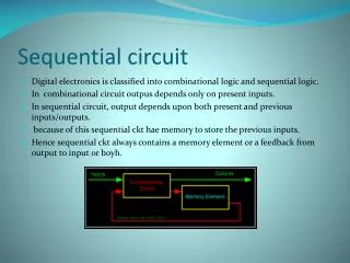
Continue… • Sequential Logic/Circuits:Latches, Flip-Flops, Triggering of Flip-Flops, Clocked Sequential Circuits and their Analysis, State Reduction and Assignment, Flip-Flop Excitation Tables, Design Procedure, Designing with D & JK Flip-Flops, HDL/Verilog Representation for a Sequential Circuits – VHDL/Verilog
Common Postulates (Boolean Algebra) • Closure N={1,2,3,4,5,…..} It is closed w.r.t + i.e. a+b=c as a,b,cΣN • Associative Law (x*y)*z = x*(y*z) for all x,y,z,ΣS • Commutative Law x*y = y*x for all x,yΣS x+y = y+x x+y = y+x x.Y = y.x
Common Postulates (Boolean Algebra) x+0 = 0+x = x x.1 = 1.x = x • Identity Element e*x = x*e = x x Σ S e+x = x+e = x 0+x = x+0 = x 1*x = x*1 = x • Inverse x*y = e a*1/a = 1 x+y = e a+(-a) = 0 • Distributed Law x*(y.z) = (x*y) . (x*z) x.(y+z) = (x.y) + (x.z) x+(y.z) = (x+y) . (x+z) x+x’ = 1 x.x’ = 0
Boolean Algebra and Logic Gates x.(y+z) = (x.y)+(x.z)
Theorems 1a. x+x = x x+x = (x+x).1 = (x+x)(x+x’) = x+xx’ =x+0 =x 1b. x.x = x (Remember Duality of 1a) x.x = xx+0 = xx+xx’ = x(x+x’) = x.1 =x
Theorems 2a. x+1 = 1 x+1 =1.(x+1) = (x+x’)(x+1) = (x+x’) = x+x’ = 1 2b. X.0 = 0 (Remember Duality of of 2a)
3. (x’)’ = x Complement of x = x’ Complement of x’ = (x’)’ = x 6a x+xy = x x+xy = x.1+xy = x(1+y) = x.1 =x 6b. x(x+y) = x (Remember Duality of 6a) Can also be proved using truth table method
x=x+xy (x+y)’ = x’y’ DeMorgan’s Theorem (xy)’ = x’ +y’ DeMorgan’s Theorem
Operator Precedence • ( ) • NOT • AND • OR
x y xy’ xy x’y x x y y x’y’ VENN DIAGRAM ILLUSTRATION X=XY+X VENN DIAGRAM FOR TWO VARIABLES x x y y z z xy+xz x+(y+z) VENN DIAGRAM ILLUSTRATION OF THE DISTRIBUTIVE LAW
TRUTH TABLE FOR F1=xyz’, F2=x+y’z, F3=x’y’z+x’yz+xy’ and F4=xy’+x’z
z F2 x x F1 y y z (b) F2 = x+y’z (a) F1 = xyz’ x y F3 z (c) F3 = x’y’z+x’yz+xy’
x y F4 (c) F4 = xy’+x’z z Implementation of Boolean Function with GATES
Algebraic Manipulations for Minimization of Boolean Functions(Literal minimization) • x+x’y = (x+x’)(x+y) = 1.(x+y)=x+y • x(x’+y) = xx’+xy = 0+xy=xy • x’y’z+x’yz+xy’ = x’z(y’+y)+xy’ = x’z+xy’ • xy+x’z+yz (Consensus Theorem) =xy+x’z+yz(x+x’) =xy+x’z+xyz+x’yz =xy(1+z)+x’z(1+y) =xy+x’z • (x+y)(x’+z)(y+z)=(x+y)(x’+z) by duality from function 4
Complement of a Function (A+B+C)’ = (A+X)’ = A’X’ = A’.(B+C)’ = A’.(B’C’) = A’B’C’ (A+B+C+D+…..Z)’ = A’B’C’D’…..Z’ (ABCD….Z)’ = A’+B’+C’+D’+….+Z’ Example using De Morgan’s Theorem (Method-1) F1 = x’yz’+x’y’z F1’ = (x’yz’+x’y’z)’ = (x+y’+z)(x+y+z’) F2 = x(y’z’+yz) F2’= [x(y’z’+yz)]’ = x’+(y+z)(y’+z’)
Example using dual and complement of each literal (Method-2) F1 = x’yz’ + x’y’z Dual of F1 = (x’+y+z’)(x’+y’+z) Complement F1’ = (x+y’+z)(x+y+z’) F2 = x(y’z’+yz) Dual of F2=x+[(y’+z’)(y+z] Complement =F2’= x’+ (y+z)(y’+z’)
Minterm or a Standard Product n variables forming an AND term provide 2n possible combinations, called minterms or standard products (denoted as m1, m2 etc.). Variable primed if a bit is 0 Variable unprimed if a bit is 1 Maxterm or a Standard Sum n variables forming an OR term provide 2n possible combinations, called maxterms or standard sums (denoted as M1,M2 etc.). Variable primed if a bit is 1 Variable unprimed if a bit is 0
FUNCTION OF THREE VARIABLES f1 = x’y’z+xy’z’+xyz =m1 + m4 + m7 f2 = x’yz+xy’z+xyz’+xyz = m3 + m5 + m6 + m7
MINTERMS AND MAXTERMS FOR THREE BINARY VARIABLES f1 = x’y’z+xy’z’+xyz f1’ = x’y’z’+x’yz’+x’yz+xy’z+xyz’ f1 =(x+y+z)(x+y’+z)(x+y’+z’)(x’+y+z’) (x’+y’+z) = M0.M2.M3.M5.M6 = M0M2M3M5M6 f2 = x’yz+xy’z+xyz’+xyz f2’ = x’y’z’+x’y’z+x’yz’+xy’z’ f2 = (x+y+z)(x+y+z’)(x+y’+z)(x’+y+z) = M0 M1 M2 M4 Canonical Form Boolean functions expressed as a sum of minterms or product of maxterms are said to be in canonical form. M3+m5+m6+m7 or M0 M1 M2 M4
Sum of Minterms (Sum of Products) Example: F = A+B’C F = A(B+B’)+B’C(A+A’) = AB+AB’+AB’C+A’B’C = AB(C+C’)+AB’(C+C’)+AB’C+A’B’C = ABC+ABC’+AB’C+AB’C’+AB’C+A’B’C = A’B’C+AB’C’+AB’C+ABC’+ABC = m1+m4+m5+m6+m7 F(A,B,C)=(1,4,5,6,7) ORing of term AND terms of variables A,B &C They are minterms of the function
Product of Maxterms (Product of sums) Example: F = xy+x’z F = xy+x’z F = (xy+x’)(xy+z) distr.law (x+yz)=(x+y)(x+z) = (x+x’)(y+x’)(x+z)(y+z) = (x’+y)(x+z)(y+z) = (x’+y+zz’)(x+z+yy’)(y+z+xx’) = (x’+y+z)(x’+y+z’)(x+z+y)(x+z+y’)(y+z+x)(y+z+x’) = (x+y+z)(x+y’+z)(x’+y+z)(x’+y+z’) = M0 M2 M4 M5 F(x,y,z) = (0,2,4,5) ANDing of terms Maxterms of the function (4 OR terms of variables x,y&z)
Conversion between Canonical Forms F(A,B,C) = (1,4,5,6,7) sum of minterms F’(A,B,C) = (0,2,3) = m0+m2+m3 F(A,B,C) = (m0+m2+m3)’ = m0’.m2’.m3’ = M0 M2 M3 = (0,2,3) Product of maxterms Similarly F(x,y,z) = (0,2,4,5) F(x,y,z) = (1,3,6,7)
Standard Forms Sum of Products (OR operations) F1 = y’+xy+x’yz’ (AND term/product term) Product of Sums (AND operations) F2=x(y’+z)(x’+y+z’+w) (OR term/sum term) Non-standard form F3=(AB+CD)(A’B’+C’D’) Standard form of F3 F3=ABC’D’ + A’B’CD
TRUTH TABLE FOR THE 16 FUNCTIONS OF TWO BINARY VARIABLES F0 = 0 F1 = xy F2 = xy’ F3 = x F4 = x’y F5 = y F6 = xy’ +x’y F7= x +y F8 = (x+y)’ F9 = xy +x’y’ F10 = y’ F11 = x +y’ F12 = x’ F13 = x’ + y F14 = (xy)’ F15 = 1
BOOLEAN EXPRESSIONS FOR THE 16 FUNCTIONS OF TWO VARIABLEBOOLEAN OPERATOR NAME COMMENTS FUNCTIONS SYMBOL F0 =0 NULL BINARY CONSTANT 0 F1=xy x.y AND x and yF2=xy’ x/y inhibition x but not y F3=x transfer x F4=x’y y/x inhibition y but not xF5=y transfer yF6=xy’+x’y x y exclusive-OR x or y but not bothF7=x+y x+y OR x or yF8=(x+y)’ x y NOR not OR F9=xy+x’y’ x y *equivalence x equals y F10=y’ y’ complement not yF11=x+y’ x y implication if y then xF12=x’ x’ complement not xF13=x’+y x y implication if x then yF14=(xy)’ x y NAND not ANDF15=1 IDENTITY BINARY CONSTANT 1
*Equivalence is also known as equality, coincidence, and exclusive NOR • 16 logic operations are obtained from two variables x &y • Standard gates used in digital design are: complement, transfer, AND, OR , NAND, NOR, XOR & XNOR (equivalence).
H and L LEVEL IN IC LOGIC FAMILIES Range Typical
TYPICAL CHARACTERISTICS OF IC LOGIC FAMILIES TTL basic circuit : NAND gate ECL basic circuit: NOR gate CMOS basic circuit: Inverter to construct NAND/NOR
DIGITAL LOGIC GATES X F Y X F Y
X F X F X F Y
F Y X F F X Y X Y
Y (X+Y)’ x [Z+(X+Y)’]’ Y (X Y) Z=(X+Y) Z’ =XZ’+YZ’ Z (X ( Y Z)=X’(Y+ Z) X =X’Y+X’Z [X+(Y+Z)’]’ (Y+Z)’ Z Demonstrating the nonassociativity of the NOR operator (X Y) Z X (Y Z)
X (XYZ)’ X (X+Y+Z)’ Y Y Z Z (a) There input NOR gate (b) There input NAND gate A B C F=[(ABC)’. (DE)’]’=ABC+DE D E (c) Cascaded NAND gates Multiple-input AND cascaded NOR and NAND gates
TRUTH TABLE X X Y Z F 0 0 0 0 1 0 0 1 1 0 0 1 0 1 0 0 1 1 0 1 1 0 0 1 0 1 0 1 0 1 1 1 0 0 1 1 1 1 1 0 Y F=X Y Z Z (a) Using two input gates XOR X Y F=X Y Z Z XNOR (b) Three input gates Odd function Even function (b) Three input exclusive OR gates
IC DIGITAL LOGIC FAMILIES TTL Transistor- Transistor Logic • Very popular logic family. • It has a extensive list of digital functions. • It has a large number of MSI and SSI devices, also has LSI devices. ECL Emitter Coupled Logic • Used in systems requiring high speed operations. • It has a large number of MSI and SSI devices, also LSI devices. MOS Metal-Oxide Semiconductor • Used in circuit requiring high component density • It has a large number of MSI and SSI devices, also LSI devices (mostly) CMOS Complementary MOS • Used in systems requiring low power consumption. • It has a large number of MSI and SSI devices, also has LSI devices. I2L Integrated - Injection Logic • Used in circuit requiring high component density. • Mostly used for LSI functions
Some Typical IC Gates VCC VCC 14 13 12 11 10 9 8 14 13 12 11 10 9 8 1 2 3 4 5 6 7 1 2 3 4 5 6 7 GND GND 7404 Hex Inverters 7400 Quadruple 2-input NAND gates TTL gates
Some Typical IC Gates VCC 2 16 15 14 13 12 11 10 9 10107 Triple Exclusive – OR/ NOR gates 1 2 3 4 5 6 7 8 VEE 2 (-5.2V) VCC 1 VCC 2 16 15 14 13 12 11 10 9 10102 Quadruple 2-Input NOR gate VEE (-5.2V) 1 2 3 4 5 6 7 8 VCC 1
(3-15 V) NC 8 VDD 14 13 12 11 10 9 C MOS GATES 1 2 3 4 5 6 NC 7 Vss (GND) 4002 dual 4 input NOR gates
NC 13 NC 16 15 14 12 11 10 9 CMOS GATES 1 VDD 2 3 5 6 7 8 Vss (GND) 4 (3-15 V) 4050 Hex buffer
SIGNAL VALUE SIGNAL VALUE LOGIC VALUE LOGIC VALUE 1 H 0 H 0 L 1 L Negative Logic Positive Logic Signal amplitude assignment and type of logic
X y z L L H L H H H L H H H L TTL 7400 GATE x z y Gate block diagram Gate block diagram Truth table in terms of H and L X y z 0 0 1 0 1 1 1 0 1 1 1 0 x z y Truth table for positive logic H=1, L=0 Graphic symbol for positive logic NAND gate
X y z 1 1 0 1 0 1 0 1 1 0 0 1 x z y Graphic symbol for negative logic NOR gate Truth table for negative logic L=1 H=0 Same gate can function +ive logic NAND or -ive logic NOR +ive logic NOR or -ive logic NAND DEMONSTRATION OF POSITIVE AND NEGATIVE LOGIC
Fan-outSpecifies the number of standard loads (the amount of current needed by an input of another gate in the same IC family) that the output of a gate can drive without impairing its normal operation. it is expressed by a number.Power dissipationIt is the supplied power required to operate the gate. It is expressed in mw.Propagation delayIt is the average transition delay time for a signal to propagate from input to output when the binary signals change in value. It is expressed in ns.Noise marginIt is the maximum noise voltage added to the input signal of a digital circuit that does not cause an undesirable change in the circuit output. It is expressed in volts (v). Characteristics of IC logic families(parameters)