Download
1 / 39
390 likes | 654 Views
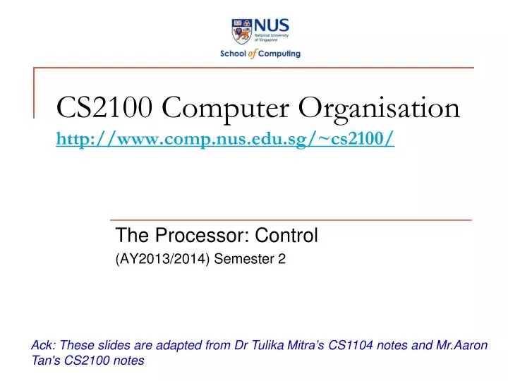
CS2100 Computer Organisation http://www.comp.nus.edu.sg/~cs2100/. The Processor: Control (AY2013/2014) Semester 2. Ack : These slides are adapted from Dr Tulika Mitra’s CS1104 notes and Mr.Aaron Tan's CS2100 notes. Road Map: Part II. Performance. Processor: Control

E N D
CS2100 Computer Organisationhttp://www.comp.nus.edu.sg/~cs2100/ The Processor: Control (AY2013/2014) Semester 2 Ack: These slides are adapted from Dr TulikaMitra’s CS1104 notes and Mr.Aaron Tan's CS2100 notes
Road Map: Part II Performance • Processor: Control • The control unit • Control Signals • ALU Control Signal Assembly Language Processor: Datapath Processor: Control Pipelining Cache Processor: Datapath
Complete Datapath Instruction Memory MUX Instruction Left Shift 2-bit Address PC PCSrc Add 4 Add ALUcontrol Inst [25:21] 4 5 RR1 RD1 5 is0? MemWrite Inst [20:16] RR2 opcode 31:26 rs 25:21 rt 20:16 rd 15:11 shamt 10:6 funct 5:0 Registers ALU ALUSrc 5 WR ALU result MUX Address MUX RD2 Data Memory MemToReg WD Inst [15:11] Read Data MUX RegWrite RegDst Write Data Sign Extend Inst [15:0] MemRead Datapath
Identified Control Signals Control
Generating Control Signals: Idea Control • The control signals are generated based on the instruction to be executed: • Opcode Instruction Format • Example: • R-Format instruction RegSrc = 1 (use Inst[15:11]) ) • R-Type instruction has additional information: • The 6-bit "funct" (function code, Inst[5:0]) field • Idea: • Design a combinatorial circuit to generate these signals based on Opcode and possibly Function code • A control unit is needed (a draft design is shown next)
The Control Unit (draft) Instruction Memory MUX Instruction Left Shift 2-bit Address Control PC PCSrc Add 4 Add ALUcontrol Inst [25:21] 4 5 RR1 RD1 5 is0? MemWrite Inst [20:16] RR2 opcode 31:26 rs 25:21 rt 20:16 rd 15:11 shamt 10:6 funct 5:0 Registers ALU ALUSrc 5 WR ALU result MUX Address MUX RD2 Data Memory MemToReg WD Inst [15:11] Read Data MUX RegWrite RegDst Write Data Sign Extend Inst [15:0] MemRead Datapath
Let's Implement the Control Unit! Control • Approach: • Take note of the instruction subset to be implemented: • Opcode and Function Code (if applicable) • Go through each signal: • Observe how the signal is generated based on the instruction opcode and/or function code • Construct truth table • Design the control unit using logic gates
opcode shamt funct 31 25 20 15 10 5 31 25 20 15 Review: MIPS Instruction Subset 016 rs rt rd 0 2016 add sub 016 rs rt rd 0 2216 rs rt rd 0 R-type 016 2416 and 016 rs rt rd 0 2516 or 016 rs rt rd 0 2A16 slt rs rd lw 2316 offset offset rd rs 2B16 sw I-type beq 416 rs rd offset Control
Control Signal: RegDst 0 MUX 1 • False (0): Write register = Inst[20:16] • True (1): Write register = Inst[15:11] Signal Control
Control Signal: RegWrite • False (0): No register write • True (1): New value will be written Control
Control Signal: ALUSrc • False (0): Operand2 = Register Read Data 2 • True (1): Operand2= SignExt(Inst[15:0]) Control
Control Signal: MemRead • False (0): Not performing memory read access • True (1): Read memory using Address Control
Control Signal: MemWrite • False (0): Not performing memory write operation • True (1): memory[Address] Register Read Data 2 Control
Control Signal: MemToReg 1 MUX 0 • True (1): Register write data = Memory read data • False (0): Register write data = ALU Result Signal IMPORTANT: The input of MUX is swapped in this case Control
Control Signal: PCSrc • The "isZero?" signal from the ALU gives us the actual branch outcome (taken / not taken) • Idea: "If instruction is a branch AND taken, then…" Control
Control Signal: PCSrc • False (0): Next PC = PC + 4 • True (1): Next PC = SignExt(Inst[15:0]) << 2 + (PC + 4) PCSrc = ( Branch ANDisZero) Control
Midpoint Check Control • We have gone through almost all of the signals: • Left with the more challenging ALUControl signal • Observation so far: • The signals discussed so far can be generated by opcode directly • Function code is not needed up to this point • A major part of the controller can be built based on opcodealone
The Control Unit v0.5 Instruction Memory PC MUX Add 4 Instruction Left Shift 2-bit Address PCSrc Control Branch Inst [31:26] Add Inst [25:21] 5 RR1 RD1 5 is0? MemWrite Inst [20:16] RR2 opcode 31:26 rs 25:21 rt 20:16 rd 15:11 shamt 10:6 funct 5:0 Registers ALU ALUSrc 5 WR ALU result MUX Address MUX RD2 Data Memory MemToReg WD Inst [15:11] 4 Read Data ALUcontrol MUX RegWrite RegDst Write Data Sign Extend Inst [15:0] MemRead
Closer Look at ALU Unit • Question: • How is the ALUcontrol signal designed? Control • The ALU Unit is a combinatorial circuit: • Capable of performing several arithmetic operations • In Lecture #14: • We noted the required operations for the MIPS subset
One Bit At A Time • 4 control bits are needed: • Ainvert: • 1 to invert input A • Binvert: • 1 to invert input B • Operation (2-bit) • To select one of the 3 results Acknowledgement: Image taken from NYU Cource CSCI-UA.0436 Control A simplified 1-bit MIPS ALU can be implemented as follows:
One Bit At A Time(A-HA!) Acknowledgement: Image taken from NYU Cource CSCI-UA.0436 Control • Can you see how the ALUcontrol (4-bits) signal controls the ALU? • Note: implementation for slt not shown
Multilevel Decoding Control • Now we can start to design for ALUcontrolsignal, which depends on: • Opcode (6-bit) and Function Code Field (6-bit) • Brute Force approach: • Use Opcode and Function Code directly, i.e. finding expressions with 12 variables • Multilevel Decoding approach: • Use some of the input to reduce the cases, then generate the full output + Simplify the design process, reduce the size of the main controller, potentially speedup the circuit
Intermediate Signal: ALUop Control • Basic Idea: • Use Opcode to generate a 2-bit ALUop signal • Represents classification of the instructions: • Use ALUop signal and Function Code field (for R-type instructions) to generate the 4-bit ALUcontrol signal
ALU 2-Level Implementation Step 1. Generate ALUop signal from 6-bit opcode. 6 Control Step 2. Generate ALUctrl signal from ALUop and optionally 6-bit Funct field. ALUop opcode 31:26 rs 25:21 2 rt 20:16 rd 15:11 shamt 10:6 funct 5:0 00: lw, sw 01: beq 10: add, sub, and, or, slt 4 ALUcontrol 0000: and 0001: or 0010: add 0110: sub 0111: set on less than ALU Control 6 Control
Generating ALUControl Signal Generation of ALUop signal will be discussed later Control
Design of ALU Control Unit (1/2) Control Input: 6-bit Funct field and 2-bit ALUop Output: 4-bit ALUcontrol Find the simplified expressions
ALUop ALUcontrol2 = ALUOp0 + ALUOp1∙F1 ALU Control block ALUOp0 (LSB) ALUcontrol3 ALUOp1 (MSB) 0 ALUcontrol2 F3 ALUcontrol ALUcontrol1 F2 F(5-0) F1 ALUcontrol0 F0 Design of ALU Control Unit (2/2) • Simple combinational logic Control
Finale: Control Design Control • We have now considered all individual signals and their expected values • Ready to design the controller itself • Typical digital design steps: • Fill in truth table • Input:Opcode • Output: Various control signals as discussed • Derive simplified expression for each signal
Datapath & Control Instruction Memory PC MUX Add 4 Instruction Left Shift 2-bit Address PCSrc Control Branch Inst [31:26] Add Inst [25:21] 5 RR1 RD1 5 is0? MemWrite Inst [20:16] RR2 opcode 31:26 rs 25:21 rt 20:16 rd 15:11 shamt 10:6 funct 5:0 Registers ALU ALUSrc 5 WR ALU result MUX Address MUX RD2 Data Memory MemToReg WD Inst [15:11] 4 Read Data ALUcontrol MUX RegWrite RegDst Write Data Sign Extend Inst [15:0] MemRead Inst [5:0] ALUop ALU Control
Control Design: Outputs Control
Control Design: Inputs Control With the input (opcode) and output (control signals), let's design the circuit
Combinational Circuit Implementation Opcode Control Signals Control Logic Control
Clock Period Clock Read Compute Write Don’t want to read a storage element when it is being written Big Picture: Instruction Execution • Instruction Execution = • Read contents of one or more storage elements (register/memory) • Perform computation through some combinational logic • Write results to one or more storage elements (register/memory) • All these performed within a clock period Control
Single Cycle Implementation: Shortcoming • Calculate cycle time assuming negligible delays except: memory (2ns), ALU/adders (2ns), register file access (1ns) • All instructions take as much time as the slowest one (i.e., load) • Long cycle time Control
Solution 1: Multicycle Implementation • Break up the instructions into execution steps: • Instruction fetch • Instruction decode and register read • ALU operation • Memory read/write • Register write • Each execution step takes one clock cycle Cycle time is much shorter, i.e., clock frequency is much higher • Instructions take variable number of clock cycles to complete execution • Not covered in class: • See Section 5.5 if interested Control
Solution 2: Pipelining • Break up the instructions into execution steps one per clock cycle • Allow different instructions to be in different execution steps simultaneously • Covered in lecture set #16 Control
Summary • A very simple implementation of MIPS datapath and control for a subset of its instructions • Concepts: • An instruction executes in a single clock cycle • Read storage elements, compute, write to storage elements • Datapath is shared among different instructions types using MUXs and control signals • Control signals are generated from the machine language encoding of instructions Control
Reading Assignments • The Processor: Datapath and Control • 3rd edition: Chapter 5 Section 5.4 • 4th edition: Chapter 4 Section 4.4 • Exploration: • ALU design and implementation: • 4th edition (MIPS): Appendix C • http://cs.nyu.edu/courses/fall11/CSCI-UA.0436-001/class-notes.html Control
End Control