Download
1 / 99
1.01k likes | 1.26k Views
Data Converter. Design Of A Wireless Sensing. Input signal Sampling rate Throughput. Resolution Range Gain. Analog to Digital (A/D) Converter. Fundamentals of Sampled Data Systems.

E N D
Input signal Sampling rate Throughput Resolution Range Gain Analog to Digital (A/D) Converter
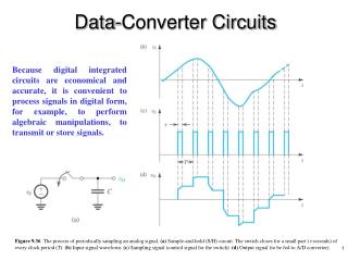
Fundamentals of Sampled Data Systems Analog-to-Digital converters (ADCs) translate analog quantities, wich are characteristic of most phenomen in the ‘’real world’’ to digital language, used in information processing, computing, data transmission, and control systems Digital-to-Analog converters (DACs) are used in transforming transmitted or stored data, or the results of digital processing, back to ‘’real world’’ variables for control, information display, or further analog processing
Digital Number Digital number used are all basically binary : that is, each ‘’bit’’ or unit of information has one of two possible states. These state are : ‘’off’’, ‘’false’’, or ‘’1’’ ‘’on’’, ‘’true’’ , or ‘’0’’ It is also possible to represent the two logic state by two different levels of current ; however, this is much less popular than using voltages . Word are groups of levels representing digital numbers; the levels may appear simultaneously in paralel , on a bus or groups of gate inputs or outputs, serially (or in time sequence) on a single line, as a sequence of parallel bytes (i.e. ‘’byte –serial’’) or nibbles (small bytes) A unique parallel or serial grouping of digital levels, or a number, or code, is assigned to each analog level which is quantized (i.e., represents a unique portion of the analog range).
Typical Digital Code A typical digital code would be this array : The meaning of the code, as either a number, a character, or a representation of an analog variable is unknow until the code and the conversion relationship have been defined
Quantization: The Size of a Least Significant Bit (LSB) The resolution of data converters
The theoretical ideal transfer function for an ADC is a straight line, however, the practical ideal transfer function is auniform staircase characteristic shown in Figure . The Ideal Transfer Function (ADC)
The DAC theoretical ideal transfer function would also be a straightline with an infinite number of steps but practically it is a series of points that fall on the ideal straight line as shown inFigure The Ideal Transfer Function (DAC)
Sources of Static Error Static errors, that is those errors that affect the accuracy of the converter when it is converting static (dc) signals, canbe completely described by just four terms. These are : Each can be expressed in LSB units or sometimes as a percentage of the FSR • offset error, • gain error, • integral nonlinearity and • differentialnonlinearity.
Offset Error - ADC Theoffset error is efined as the difference between the nominal and actual offset points.
For a DAC it is the step value when thedigital input is zero. This error affects all codes by the same amount and can usually be compensated for by a trimmingprocess. If trimming is not possible, this error is referred to as the zero-scale error. Offset Error - DAC
The gain error is defined as the difference between the nominal and actual gain points on the transferfunction after the offset error has been corrected to zero. For an ADC, the gain point is the midstep value when the digitaloutput is full scale, Gain Error - ADC
For a DAC it is the step value when the digital input is full scale. This error represents a differencein the slope of the actual and ideal transfer functions This error can also usually be adjusted to zero by trimming. Gain Error - DAC
DNL is the differencebetween an actual step width (for an ADC) and the ideal value of 1 LSB. Therefore if thestep width is exactly 1 LSB, then the differential nonlinearity error is zero. If the DNL exceeds 1 LSB nonmonotonic (this means that the magnitude of the output gets smallerfor an increase in the magnitude of the input) If theDNL error of – 1 LSB there is also a possibility that there can be missing codes i.e.,one or more of the possible 2n binary codes are never output. Differential Nonlinearity (DNL) Error - ADC
The differential nonlinearity error shown in Figure is the differencebetween an actual step height (for a DAC) and the ideal value of 1 LSB. Therefore if thestep height is exactly 1 LSB, then the differential nonlinearity error is zero Differential Nonlinearity (DNL) Error - DAC
The integral nonlinearity error shown in Figure is the deviation of the valueson the actual transfer function from a straight line. This straight line can be either a best straight line which is drawn soas to minimize these deviations or it can be a line drawn between the end points of the transfer function once the gainand offset errors have been nullified (end-point linearity ) Integral Nonlinerity (INL) Error - ADC
Integral Nonlinerity (INL) Error - DAC - The name integral nonlinearity derives from the fact that the summation of the differential nonlinearitiesfrom the bottom up to a particular step, determines the value of the integral nonlinearity at that step.
The absolute accuracy or total error of an ADC as shown in Figure is the maximum value of the difference betweenan analog value and the ideal midstep value. It includes offset, gain, and integral linearity errors and also the quantizationerror in the case of an ADC Absolute Accuracy (Total) Error -ADC-
Prior to the actual analog-to-digitalconversion, the analog signal usually passes through some sort of signal conditioningcircuitry which performs such functions as amplification, attenuation, and filtering. Thelowpass/bandpass filter is required to remove unwanted signals outside the bandwidth ofinterest and prevent aliasing. There are two key concepts involved in the actual analog-to-digital and digital-to-analogconversion process: An understanding of these concepts is vital to data converter applications. Sampling Theory • discrete time sampling and • finite amplitude resolution due toquantization.
The system shown in Figure is real-time system ; i.e., the signal to the ADC is continuously sampled at a rate equal to fS, and the ADC presents a new sample to the DSP at this rate. In order to maintain real-time operation, the DSP must perform all its required computation within the sampling interval, 1/fS, and present an output sample to the DAC beforearrival of the next sample from the ADC. Sampling Theory
The Need for a Sample-and-Hold Amplifier (SHA) Function Most ADCs today have abuilt-in-sample-and-hold function, thereby allowing them to process ac signals. This type of ADC is referred to as a sampling ADC If the input signal to a SAR ADC (assuming no SHA function) changes by more than 1LSB during the conversion time (8ms is the example), the output data can have large errors, depending on the location of the code Most ADC architectures are subject to this type of error – some more, some less – with the possible exception of flash converters having well-matched comparators
Input Frequency Limitations of Nonsampling ADC (Encoder) This implies any input frequency greater than 9.7 Hz is subject to conversion errors, even though a sampling frequency of 100 kSPS is possible with the 8ms ADC (this allows an extra 2ms interval for an external SHA to reacquire the signal after coming out of hold mode).
Sample-and-Hold Function Required for Digitizing AC Signals Sample-and-hold amplifier (SHA) Track-and-hold amplifier (THA).
A continuous analog signal is sampled at discrete intervals, fS,which must be carefully chosen to ensure an accurate representation of the original analog signal The Nyquist criteria requiries that the sampling frequency be at least twice the highest frequency contained in the signal, or information about the signal will be lost If the sampling frequency is less than twice the maximum analog signal frequency, a phenomen know as aliasing will occur The Nyquist Criteria • A signal with a maximum frequency .. must be sampled at a rate .... or information about the signal will be lost because of aliasing • Aliasing occurs whenever ... • A signal which has frequency components between .. and.... must be sampled at a rate ...... in order to prevent alias components from overlapping the signal frequencies
Aliasing in Time Domain In order to understand the implications of aliasing in both the time and frequency domain, first consider the case of a time domain representation of a single tone sinewavesampled as shown in Figure
Consider the case of a single frequency sinewave of frequency fa sampled at a frequency fs by an ideal impulse sampler. Also assume that fs > 2faas shown. The frequency-domain output of the sampler shows aliases or imagesof the original signal around every multiple of fs, i.e. at frequencies equal to |± Kfs ± fa|, K = 1,2, 3, 4, ..... Aliasing in Frequency Domain
Baseband sampling implies that the signal to be sampled lies in the first Nyquist zone. Itis important to note that with no input filtering at the input of the ideal sampler, anyfrequency component (either signal or noise) that falls outside the Nyquist bandwidth inany Nyquist zone will be aliased back into the first Nyquist zone. For this reason, anantialiasing filter is used in almost all sampling ADC applications to remove theseunwanted signals. The antialiasing filter transition band is therefore determined by the corner frequency fa,the stopband frequency fs – fa, and the desired stopband attenuation, DR. The requiredsystem dynamic range is chosen based on the requirement for signal fidelity. For instance, a Butterworth filter gives 6-dB attenuation per octave for each filter pole (as do all filters). Achieving 60 dB attenuation in a transition region between 1MHz and 2 MHz (1 octave) requires a minimum of 10 poles—not a trivial filter, anddefinitely a design challenge. Baseband Antialiasing Filter
Oversampling RelaxesRequirementson Baseband Antialiasing Filter The effects of increasing the samplingfrequency by a factor of K, while maintaining the same analog corner frequency, fa, andthe same dynamic range, DR, requirement. The wider transition band (fa to Kfs – fa)makes this filter easier to design
Comparing a Nyquist rate (a) and Oversampling strategies (b)
The only errors (dc or ac) associated with an ideal N-bit data converter are those relatedto the sampling and quantization processes. The maximum error an ideal converter makeswhen digitizing a signal is ±½ LSB. The transfer function of an ideal N-bit ADC isshown in Figure Data Converter AC Error
FFT diagram of a multi-bit ADC with a sampling frequency FS This noise is approximately Gaussian and spreadmore or less uniformly over the Nyquist bandwidth dc to fs/2.
Theoretical Signal-to-Quantization Noise Ratioof an Ideal N-Bit Converter
In many applications, theactual signal of interest occupies a smaller bandwidth, BW. If digital filtering is used tofilter out noise components outside the bandwidth BW, then a correction factor (calledprocess gain) must be included in the quation to account for the resulting increase inSNR. Procces Gain
Probably the most significant specification for an ADC used in a communications application is its spurious free dynamic range (SFDR). SFDR of an ADC is defined asthe ratio of the rms signal amplitude to the rms value of the peak spurious spectralcontentmeasured over the bandwidth of interest. SFDR is generally plotted as a function of signal amplitude and may be expressed relative to the signal amplitude (dBc) or the ADC full-scale (dBFS) as shown in Figure Spurious Free Dynamic Range (SFDR)
Design a Low-Jitter Clock for High-Speed Data Converter Many modern, high speed, high performance IC’s ADC’s require a low-phase-noise (low-jitter) clock that operates in the GHz range Conventional crystal oscillators may provide a low jitter clock signal, but are not generally available in oscilating frequencies above 120 MHz Typical high-speed data converter system
Jitter in clock signal degrades the ADC signal-to-noise ratio. Jitter is generally defined as short-term, non-cumulative variation ofthe significant instant of a digital signal from its ideal position in time. Figure illustrates asampling clock signal that contains jitter. Jitter generated by the clock is caused by variousinternal noise sources, such as thermal noise, phase noise, and spurious noise. A clock signal that has cycle-to-cycle variation in its duty cycle is said to exhibit jitter. Clock jittercauses an uncertainty in the precise sampling time, resulting in a reduction of dynamic performance.