Download

1 / 9
90 likes | 239 Views
EE- 584 DESIGN AND TESTING OF A CMOS INVERTER. LAKSHMAN KUMAR GOKAVARAPU. OBJECTIVE : Design and test the working of an inverter using Mentor graphics Software. STEPS ADOPTED : 1) Design of schematic using Design Architect

E N D
EE- 584 DESIGN AND TESTING OF A CMOS INVERTER LAKSHMAN KUMAR GOKAVARAPU
OBJECTIVE : Design and test the working of an inverter using Mentor graphics Software. STEPS ADOPTED : 1) Design of schematic using Design Architect 2) Testing the functionality of schematic using quicksim. 3) Design of Layout corresponding to schematic using IC workstation. 4) Verification of Layout using DRC rules LVS report. 5) Parameter extraction using IC extract. 6) Testing the functional correctness of Layout using accusim.
TRUTH TABLE Schematic of inverter Fig.1
Symbol of inverter Fig.2 Quicksim Simulation Results Fig.3
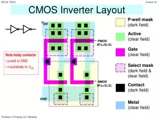
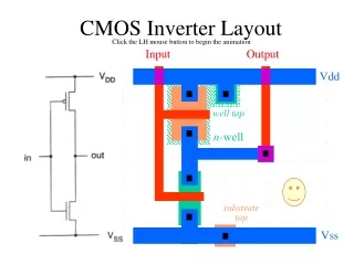
Layout Fig.4
DRC rules: Define the spacing between various layers , which should be followed during designing a layout. The following are some of the rules: 1) 2-Minimum width of poly. 2) 2-Minimum width and length of contact. 3) 2-Minimum extension of poly beyond diff. 4) 1.5-Minimum enclosure of contact by diff. 5) 2-Minimum spacing between contact and poly. 6) 3-Minimum poly-poly interspacing. LVS Report : The layout versus schematic tool (LVS) checks whether the layout matches with the schematic in terms of number of ports and instances.
Fig.5 PARAMETER EXTRACTION : Done to extract and back annotate the lumped parameters. The value of the lumped parameters including intrinsic capacitances could be obtained.
Accusim Results Fig.6
Conclusions:CMOS inverter was designed using Mentor Graphics tool. The layout was designed with minimum total area and the inverter was verified for its functionality.