Download
1 / 27
280 likes | 519 Views
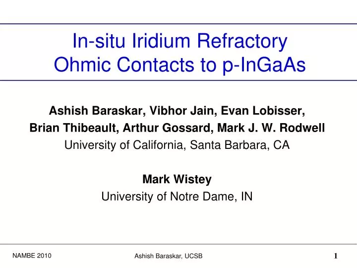
In-situ Iridium Refractory Ohmic Contacts to p-InGaAs. Ashish Baraskar, Vibhor Jain, Evan Lobisser, Brian Thibeault, Arthur Gossard, Mark J. W. Rodwell University of California, Santa Barbara, CA Mark Wistey University of Notre Dame, IN. Outline. Experimental details Contact formation

E N D
In-situ Iridium Refractory Ohmic Contacts to p-InGaAs Ashish Baraskar, Vibhor Jain, Evan Lobisser, Brian Thibeault, Arthur Gossard, Mark J. W. Rodwell University of California, Santa Barbara, CA Mark Wistey University of Notre Dame, IN
Outline • Experimental details • Contact formation • Fabrication of Transmission Line Model structures • Motivation • Low resistance contacts for high speed HBTs • Approach • Results • Doping characteristics • Effect of doping on contact resistivity • Effect of annealing • Conclusion
Outline Motivation Low resistance contacts for high speed HBTs Approach • Experimental details • Contact formation • Fabrication of Transmission Line Model structures • Results • Doping characteristics • Effect of doping on contact resistivity • Effect of annealing • Conclusion
Device Bandwidth Scaling Laws for HBT To double device bandwidth: • Cut transit time 2x • Cut RC delay 2x Scale contact resistivities by 4:1* HBT: Heterojunction Bipolar Transistor *M.J.W. Rodwell, CSICS 2008
InP Bipolar Transistor Scaling Roadmap Contact resistivity serious challenge to THz technology Less than 2.5 Ω-µm2 base contact resistivity required for simultaneous THz ft and fmax* *M.J.W. Rodwell, CSICS 2008
Approach - I To achieve low resistance, stable ohmic contacts • Higher number of active carriers - Reduced depletion width - Enhanced tunneling across metal- semiconductor interface • Better surface preparation techniques - For efficient removal of oxides/impurities
Approach - II • Scaled device thin base (For 80 nm device: tbase < 25 nm) • Non-refractory contacts may diffuse at higher temperatures through base and short the collector • Pd/Ti/Pd/Au contacts diffuse about 15 nm in InGaAs on annealing Need a refractory metal for thermal stability 15 nm Pd/Ti diffusion 100 nm InGaAs grown in MBE TEM: Evan Lobisser
Outline Motivation Low resistance contacts for high speed HBTs and FETs Approach • Experimental details • Contact formation • Fabrication of Transmission Line Model structures • Results • Doping characteristics • Effect of doping on contact resistivity • Effect of annealing • Conclusion
Epilayer Growth 100 nm In0.53Ga0.47As: C (p-type) 100 nm In0.52Al0.48As: NID buffer Semi-insulating InP Substrate Epilayer growth by Solid Source Molecular Beam Epitaxy (SS-MBE)– p-InGaAs/InAlAs - Semi insulating InP (100) substrate - Un-doped InAlAs buffer - CBr4 as carbon dopant source - Hole concentration determined by Hall measurements
In-situ Ir contacts 20 nm in-situ Ir 100 nm In0.53Ga0.47As: C (p-type) 100 nm In0.52Al0.48As: NID buffer Semi-insulating InP Substrate In-situ iridium (Ir) deposition • E-beam chamber connected to MBE chamber • No air exposure after film growth Why Ir? • Refractory metal (melting point ~ 2460 oC) • Easy to deposit by e-beam technique • Easy to process and integrate in HBT process flow
50 nm ex-situ Ni 500 nm ex-situ Au 20 nm ex-situ Ti 20 nm in-situ Ir 100 nm In0.53Ga0.47As: C (p-type) 100 nm In0.52Al0.48As: NID buffer Semi-insulating InP Substrate TLM (Transmission Line Model) fabrication • E-beam deposition of Ti, Au and Ni layers • Samples processed into TLM structures by photolithography and liftoff • Contact metal was dry etched in SF6/Ar with Ni as etch mask, isolated by wet etch
Resistance Measurement • Resistance measured by Agilent 4155C semiconductor parameter analyzer • TLM pad spacing (Lgap) varied from 0.5-25 µm; verified from scanning electron microscope (SEM) • TLM Width ~ 25 µm
Error Analysis • Processing errors: • Variable gap spacing along width (W) • Overlap resistance Variable gap along width (W) 1.10 µm 1.04 µm Lgap dR dd W Overlap Resistance dRc • Extrapolation errors: • 4-point probe resistance measurements on Agilent 4155C • Resolution error in SEM
Outline Motivation Low resistance contacts for high speed HBTs and FETs Approach • Experimental details • Contact formation • Fabrication of Transmission Line Model structures • Results • Doping characteristics • Effect of doping on contact resistivity • Effect of annealing • Conclusion
Doping Characteristics-I • Hole concentration saturates at high CBr4 fluxes • Number of di-carbon defects as CBr4 flux * Hole concentration Vs CBr4 flux Tsub = 460 oC *Tan et. al. Phys. Rev. B 67 (2003) 035208
Doping Characteristics-II As V/III ratio hole concentration Hole concentration Vs V/III flux CBr4 = 60 mtorr hypothesis: As-deficient surface drives C onto group-V sites
Tendency to form di-carbon defects as Tsub * Doping Characteristics-III Hole concentration Vs substrate temperature CBr4 = 60 mtorr *Tan et. al. Phys. Rev. B 67 (2003) 035208
Tendency to form di-carbon defects as Tsub * Doping Characteristics-III Hole concentration Vs substrate temperature CBr4 = 60 mtorr *Tan et. al. Phys. Rev. B 67 (2003) 035208
Results: Contact Resistivity - I • Hole concentration, p = 2.2 x 1020 cm-3 • Mobility, µ = 30 cm2/Vs • Sheet resistance, Rsh = 94 ohm/ (100 nm thick film) ρc lower than the best reported contacts to pInGaAs (ρc= 4 Ω-µm2)[1,2] 1. Griffith et al, Indium Phosphide and Related Materials, 2005. 2. Jain et al, IEEE Device Research Conference, 2010.
Results: Contact Resistivity - II Tunneling Thermionic Emission rc ~ constant* p = 5.7×1019 cm-3 p = 2.2×1020 cm-3 Data suggests tunneling High active carrier concentration is the key to low resistance contacts * Physics of Semiconductor Devices, S M Sze
Thermal Stability - I Mo contacts annealed under N2 flow for 60 mins. at 250 oC TEM: Evan Lobisser
Summary • Maximum hole concentration obtained = 2.2 x1020 cm-3 at a substrate temperature of 350 oC • Low contact resistivity with in-situ Ir contacts lowest ρc= 0.58 ± 0.48 Ω-µm2 • Need to study ex-situ contacts for application to HBTs
Thank You ! Questions? Acknowledgements: ONR, DARPA-TFAST, DARPA-FLARE
Correction for Metal Resistance in 4-Point Test Structure I V V I Error term (Rmetal/x) from metal resistance
Random and Offset Error in 4155C • Random Error in resistance measurement ~ 0.5 mW • Offset Error < 5 mW* *4155C datasheet
Accuracy Limits • Error Calculations • dR = 50 mΩ (Safe estimate) • dW = 1 µm • dGap = 20 nm • Error in ρc ~ 40% at 1.1 Ω-µm2