Download
1 / 41
420 likes | 618 Views
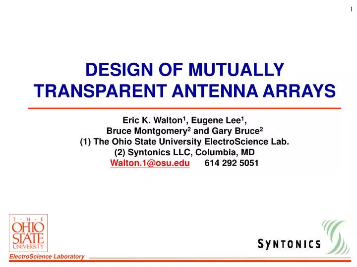
DESIGN OF MUTUALLY TRANSPARENT ANTENNA ARRAYS. Eric K. Walton 1 , Eugene Lee 1 , Bruce Montgomery 2 and Gary Bruce 2 (1) The Ohio State University ElectroScience Lab. (2) Syntonics LLC, Columbia, MD Walton.1@osu.edu 614 292 5051. BASIC CONCEPT OF THE FSS ARRAY ANTENNA CLUSTER.

E N D
DESIGN OF MUTUALLY TRANSPARENT ANTENNA ARRAYS Eric K. Walton1, Eugene Lee1, Bruce Montgomery2 and Gary Bruce2 (1) The Ohio State University ElectroScience Lab. (2) Syntonics LLC, Columbia, MD Walton.1@osu.edu 614 292 5051
BASIC CONCEPT OF THE FSS ARRAY ANTENNA CLUSTER BEAM 1 BEAM 2 BEAM 3 ARRAY 2 ARRAY 1 RADOME ARRAY 3 MECHANICALLY STEERED BEAMS MUTUALLY TRANSPARENT ANTENNA ARRAYS MOUNTED INSIDE A RADOME
BASIC ARRAY CONCEPT EACH TRANSPARENT ANTENNA PANEL: STYROFOAM DIELECTRIC RADIATING ELEMENTS PRINTED ON MYLAR FSS TRANSMISSION LINES PRINTED ON DUROID FSS GROUND PLANE PRINTED ON MYLAR EACH OUTER ARRAY ANTENNA IS TRANSPARENT TO THE INNER ARRAYS
MUTUALLY TRANSPARENT FSS ARRAY ANTENNAS TRANSMISSION LINE DESIGN AND TESTING
Center part of layout; view from top This layout is only so that the basic repeating pattern can be understood. Red = transmission lines Yellow = slots in foam Gray = holes in foam/Mylar Green = FSS pattern on Mylar (ant. Elements not shown)
RF Transparent Array Antenna for Dense Array Cluster Branch lines Main trunk line Proportional power directional couplers Rotating element feed stubs The transmission line array was perhaps the most complex part of the entire system.
Radiating CP dipoles FSS Ground Plane Transmission Line TRANSMISSION LINE LOCATION GAP “D”
MUTUALLY TRANSPARENT FSS ARRAY ANTENNAS RADIATING ELEMENT DESIGN AND TESTING
Comparison of Element Designs Cut Corners Concave Corners • Element Radius = 0.45λ (0.079m) • Single Loop Circumference = 1.33λ (0.236m) • Zin @ 1697 MHz = 90.691 – j 2.039 Ω • Element Radius = 0.45λ (0.079m) • Single Loop Circumference = 1.40λ (0.248m) • Zin @ 1697 MHz = 90.959 – j 2.387 Square Corners (original element) • Element Radius = 0.52λ (0.092m) • Single Loop Circumference = 1.40λ (0.248m) • Zin @ 1697 MHz = 61.268 – j 8.959 Ω
S-band Arrays • Single element side length and break position was optimized for peak gain at resonance (see appended slides) • 14x14 array simulated over ‘+x+x+’ FSS ground planes of different sizes (results on following three slides) s Figure 1: Sample S-band Element (side length, s = 0.34λ2230MHz; break position = 2/3) Figure 2: Sample FSS Configuration
Dual Rhombic Loop • Length of side = 0.354λ = 62.58 mm • Size of break = 0.016λ = 2.82 mm • Size of connector = 8 mm • Resonant Frequency = 1697MHz • Input Impedance = 61.914 + j 0.080773 Ω • Max gain = 3.888 dBi
RF Transparent Array Antenna for Dense Array Cluster Flat loop antenna
RF Transparent Array Antenna for Dense Array Cluster TESTING THE FLAT LOOP ANTENNA Abused (cold) grad students: Eugene Lee (PHD) And Ryan Pavlovicz (Senior – soon to be grad student)
MUTUALLY TRANSPARENT FSS ARRAY ANTENNAS FSS GROUND PLANE DESIGN AND TESTING
FSS GROUND PLANE PRINTED ON MYLAR RADIATING ELEMENTS AND FSS GROUND PLANE ARE MADE OF COPPER OR SILVER PRINTED ON MYLAR DIELECTRIC SUBSTRATE IS SIMPLY A PANEL OF STYROFOAM (THE MYLAR LAYERS GIVE IT STRENGTH AND RIGIDITY) THE TRANSMISSION LINE STRUCTURE IS TWIN LINES PRINTED ON STABLE DIELECTRIC
MUTUALLY TRANSPARENT FSS ARRAY ANTENNAS FULL SYSTEM DESIGN AND TESTING
FULL SYSTEM MODELING RADIATING ELEMENTS; FSS LAYER; TRANSMISSION LINE SYSTEM EXAMPLE; WIRE GRID MODEL OF L-BAND ARRAY BLOCKING S-BAND ARRAY
MODELING RESULTS S-band Octagonal Array • 156 Elements • Input impedance ~ 103.7 + j17.6Ω • Boresite gain = 31.9 dBiC • 162 x 152 FSS ground plane
S-Band Boresight gain vs. frequency for individual quadrants
CR BLOCKAGEExperimental Setup Walton (not to scale) These are foam panels (25 lbs or less) 4.25” thick; 84” diameter - octagonal Range center line Eugene’s Slide ~(12’ x 6’ x 5”) 84” Support Legs Foam (or other EM transparent Support columns (built by J. Moncrief)
ANALYSIS OF EXPERIMENTAL TESTING S band array at boresight vs. L band array blockage Percent blockage results GAIN (DBIC) VS. FREQ. (MHZ)
S band array patterns @ 2170 MHzfor different blockage % GAIN (DBIC) -40 -30 -20 -10 0 10 20 S band blocked by L-band array NO; EDGE; 25%; 50%; 75%; 100% -80 -60 -40 -20 0 20 40 60 80 AZIMUTH (DEG)
S band array patterns @ 2170 MHzfor different occlusion % [zoom] ZOOM GAIN (DBIC) -40 -30 -20 -10 0 10 20 S band blocked by L-band array NO; EDGE; 25%; 50%; 75%; 100% -25 -20 -15 -10 -5 0 5 10 15 20 25 AZIMUTH (DEG)
S band array patterns @ 2170 MHzfor different occlusion % [zoom 2x] ZOOM GAIN (DBIC) 8 10 12 14 16 18 20 S band blocked by L-band array NO; EDGE; 25%; 50%; 75%; 100% -5 -4 -3 -3 -1 0 1 2 3 4 5 AZIMUTH (DEG)
MORE INFORMATION AVAILABLE (much more) • Dr. Eric K. Walton The Ohio State Univ. ElectroScience Lab Columbus, OH; walton.1@osu.edu 614 292 5051 • Mr. Bruce Montgomery President; Syntonics LLC Columbia, MD bruce.montgomery@syntonicscorp.com 410/884-05800 x 201 www.syntonicscorp.com
PROTOTYPE READY FOR TESTING PROTOTYPE INTEGRATION: SUPPORT MECHANISM POSITIONING MECHANISM EM TRANSPARENT ARMS BEAMS ARE STEERED USING ONLY LOW-POWER SERVOMECHANISMS
Calibrated S band Boresight Gain Measurementsoutdoor ~17.3 dBiL
As expected Full Array gain study Too low In tracking down where the 10 dB went, we discovered that the silver printed on Mylar had slowly oxidized. Both the FSS ground plane elements and the radiating elements were now resistive. (20 to 50 ohms end-to-end!)
RESEARCH SO FAR • WE ACTUALLY BUILT AND TESTED A 3-ANTENNA SYSTEM! • PARTNERS: (SBIR PHASE 1 AND 2) (PHASE 3 HOPEFUL) • SPAWAR SAN DIEGO • THE OSU ELECTROSCIENCE LAB. (ERIC WALTON) • SYNTONICS LLC (BRUCE MONTGOMERY) • PROBLEMS OVERCOME: (DESIGN, CONSTRUCTION , TESTING) • EM TRANSPARENT RADIATING ELEMENTS • EM TRANSPARENT FSS GROUND PLANE • EM TRANSPARENT DIELECTRIC SUPPORT PANEL • EM TRANSPARENT TRANSMISSION LINE FEED SYSTEM • EM TRANSPARENT SUPPORT ARMS • EM TRANSPARENT PANEL SUPPORT STEERING MECHANISM/CONTROL • TEST AND EVALUATION PROCESS AND IT WORKED VERY WELL (GAIN; SIDELOBES; POLARIZATION; MUTUAL INDEPENDENCE)
FUTURE RESEARCH NEEDED: • (6.1 research program) • GENERALIZE THE DESIGN OF FSS TRANSMISSION LINE FEED NETWORKS (this is a PHD problem & is now in progress) • GENERALIZE THE DESIGN OF THE MULTIPLE ARRAY SYSTEM (other groups will need to do their own specialized designs) • (6.2 research program) • OPTIMIZE THE DESIGN OF THE SYSTEM COMPONENTS (ELEMENTS, FSS, TRANSMISSION LINES) (better & lower cost components, interconnections and structural supports to be developed) • OPTIMIZE THE PRINTING OF COPPER OR SILVER LINES ON MYLAR (practical chemistry problems to be overcome) • OPTIMIZE THE INTEGRATION OF THE “STACK” (better materials, low dielectric adhesives, interconnections between printed conductive lines and the transmission line network, possible spherical segment shapes for arrays) • (6.3 research program) • BUILD AND TEST A FULLY OPERATIONAL PROTOTYPE SYSTEM (demonstrate tracking of multiple satellites; provide operational data) • DEVELOP LOW COST AND EFFECTIVE MANUFACTURING PROCESSES FOR HIGH VOLUME PRODUCTION (possibly in partnership with larger manufacturing corporation)