Download
1 / 10
100 likes | 286 Views
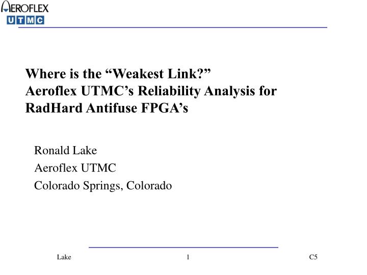
Where is the “Weakest Link?” Aeroflex UTMC’s Reliability Analysis for RadHard Antifuse FPGA’s. Ronald Lake Aeroflex UTMC Colorado Springs, Colorado. Overview. RadHard FPGA Design For Reliability Unprogrammed and Programmed FPGA Characterization SEL / SEU Analysis Design Plan

E N D
Where is the “Weakest Link?”Aeroflex UTMC’s Reliability Analysis for RadHard Antifuse FPGA’s Ronald Lake Aeroflex UTMC Colorado Springs, Colorado Lake
Overview • RadHard FPGA Design For • Reliability • Unprogrammed and Programmed FPGA • Characterization • SEL / SEU Analysis • Design Plan • Create Series of Designs to Control and Observe Key Features For Test • Design Should Isolate FPGA Resources for Analysis • Verify Characteristics in Silicon, Not Simulation • Utilize Mixed Schematic and Verilog Design Entry • Partially Control Place and Route to Force Utilization of Desired Vialinks to Evaluate Antifuse Reliability Lake
S D CK R Review FPGA Logic Cell Prior to Design QS A1 A2 A3 AZ A4 A5 A6 OS OP OZ B1 B2 C1 S C2 MP D QZ MS D1 CK D2 R E1 E2 NP NZ NS F1 F2 FZ F3 F4 F5 F6 Q2Z PS PP QC DCLK CLKSEL QR GRST Lake
IP 24 1,536 RAM High Speed Blocks Logic Cells Interface Review FPGA Cell Resources Prior to Design Lake
Reliability Design • Requires • High Gate and Wiring Utilization • Full RAM Utilization • “Easy to Test” Design Structures: • Combinatorial Blocks • Register File • Shift Register • Counters • BIST for RAM • Used for • FIT • Burn-In • Life Test • Total Ionizing Dose • Dose Rate Lake
Reliability Design +++++++++++++++++++++++++++ | Utilization Information | +++++++++++++++++++++++++++ Utilized cells (no buffers): 1536 of 1536 (100.0%) Utilized cells (buffered): 1536 of 1536 (100.0%) Utilized Logic cell Frags (no buffers): 6698 of 9216 (72.7%) Utilized Logic cell Frags (buffered): 6945 of 9216 (75.4%) Utilized Fragment A : 1162 Utilized Fragment F : 1162 Utilized Fragment O : 1536 Utilized Fragment N : 1536 IO control cells: 10 of 16 (62.5%) Clock only cells: 5 of 9 (55.6%) Bi directional cells: 95 of 99 (96.0%) RAM cells: 24 of 24 (100.0%) PLL cells: 0 of 4 (0.0%) Flip-Flop of IO cells: 32 of 315 (10.2%) 1st Flip-Flop of Logic cells: 651 of 1536 (42.4%) 2nd Flip-Flop of Logic cells: 652 of 1536 (42.4%) Routing resources: 59974 of 119431 (50.2%) ViaLink resources: 53237 of 3213992 (1.7%) Lake
Characterization Design • Requires • Ability to Isolate, Control and Observe Key Structures • All I/O Types (LVTTL, LVCMOS, PCI, GTL+, SSTL2, SSTL3) • I/O Register Cells • JTAG • Logic Cell Combinatorial Fragments • Logic Cell Registers • Memory Cells • Counters with Dedicated Clock and High Drive Clock Inputs • Heavily Loaded Dedicated Clock and High Drive Inputs • Used for • Voltage / Current Characterization on I/O • Timing Characterization • Slew Rate Analysis of Outputs • Noise Test Lake
SEL / SEU Design • Requires • High Utilization of Logic Cell Flip-Flops • Register File • Shift Registers With / Without Combinatorial Logic • High Utilization of I/O Cell Flip-Flops • Capture and Hold Input / Output Data • Full RAM Utilization • Draws From Expertise at Aeroflex UTMC in Heavy Ion Testing • Used for • SEL • SEU Lake
Lessons Learned • K.I.S.S O.F.F.- Keep It Simple Stupid (Or Face Failure) • Coordinate Design with Test and Product Engineering • Design What You Can Test in the Real World • Isolate, Control and Observe • Study FPGA Logic Cell, Overall FPGA Resources and Clock Networks Prior to Design • Registers in I/O Buffers • RAM • Dedicated and Programmable Clocks, High Drive I/O Controls Lake
Lessons Learned • Closely Review Results of Synthesis (for HDL Code), Logic Optimization and Technology Mapping • Use Schematic Capture to Implement Specific Gate Structures • Use HDL Language for Large Repetitive Structures • Use Place and Route Tools to Hand Layout Critical Circuits • Use Extreme Care With Multiple Clock Domains • If At All Possible, Use Dedicated Clock Distribution Tree • Multiple Clock Domains Lessen Efficiency of Place and Route (Technology Mapper) • Use Programmable Clocks and High Drive I/O Controls for Distributed Control Signals (Resets, Sets, Output Enable) Lake