Download
1 / 38
380 likes | 489 Views
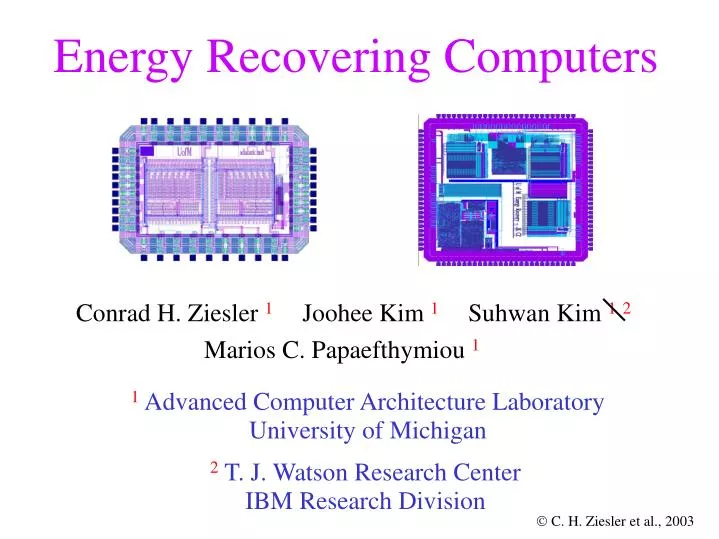
1 Advanced Computer Architecture Laboratory University of Michigan. Energy Recovering Computers. Conrad H. Ziesler 1 Joohee Kim 1 Suhwan Kim 1 2 Marios C. Papaefthymiou 1. 2 T. J. Watson Research Center IBM Research Division. P R. Vdd. V R. V C. I R. E R. Conventional CMOS Operation.

E N D
1 Advanced Computer Architecture Laboratory University of Michigan Energy Recovering Computers Conrad H. Ziesler1Joohee Kim1Suhwan Kim12 Marios C. Papaefthymiou1 2 T. J. Watson Research Center IBM Research Division
PR Vdd VR VC IR ER Conventional CMOS Operation R Vdd _ + C R Vss time • Constant supply voltage • One-way street to ground • High voltage drops across conducting devices • Energy dissipation grows with CV2
Vdd Vpc VC VR PR IR ER Charge Recovery R Vpc ~ C time • Time-varying voltage supply Vpc • Charge recovered from load C • Charge transfer through resistor is spread over available time • Energy dissipation grows with (RC/T) CV2
Quick Glance at History • Physics (1970s) • Logical reversibility of computation • Connection to thermodynamics (“adiabatic” computing) • No absolute minimum to energy dissipation, if computing is arbitrarily slow. (Does not have to be slow, however.) • Engineering (1990s) • Logic circuitry • Energy recycling circuitry • VLSI prototyping
Complex web of intertwined issues 1. Which capacitance to recover from? 2. How to store/reuse recovered energy? 3. What circuits to do the recovery? The Design Space 3. 1. 2.
The case for reversible computation P. Solomon and D. Frank – SLPE'94 Asymptotically zero-energy split-level charge recovery logic S.G. Younis and T. F. Knight, Jr. – SPLE’94 Clock-powered CMOS: A hybrid adiabatic logic style for energy-efficient computing N. Tzartzanis and W. C. Athas – ARVLSI'99 And many, many others.... Few real working chips, however. Sample Design Points from’90s
Our Contributions • Multiplier chip (2001) • Custom dynamic circuitry with fine-grain recovery from outputs of • individual gates • Discrete wavelet transform chip (2003) • Standard-cell ASIC design with recovery of clock power • Guiding principles • Simplicity • Minimal control and hardware overhead • Key attributes • Single-phase sinusoidal waveform for power and synchronization • Integrated power-clock generators with inductive elements • Relatively high operating speeds (200MHz+ in silicon) • Higher energy efficiency than conventional counterparts
Multiplier Chip • Suhwan Kim (while still at UM) and Conrad Ziesler received First Prize in VLSI Design Contest, DAC 2001. • Minimalist approach • Simple tools: magic and spice • Low-cost standard CMOS process: • HP 0.5mm, 40-pin DIP package, through MOSIS. • Operational chip demonstrates practicality of energy-recovering circuit design • Non-trivial size (8-bit operands, on-chip clock, self-test) • High throughput • Low energy dissipation
Low-Energy High-Speed Operation • Working 1st silicon • Simple yet effective experimental setup. • Correct operation verified @ 130 MHz. • Energy efficient operation validated by measurements.
Correct Function 130MHz signature output
Energy Comparison 2 stage static CMOS 500 2.9V 4 stage static CMOS 8 stage static CMOS Energy recovery 400 3.0V 3.0V 4x 300 Dissipation per Cycle (pJ) 1.9V 200 1.6V 2.3V 2.0V 100 2.7V 1.9V 2.2V 0 50 140 100 200 Frequency (MHz)
Simulations vs. Measurements 80 60 Discrepancy (%) 40 20 0 40 50 60 70 90 100 110 120 130 Frequency (MHz) • Good correspondence up to 100MHz • Simulations gave consistently higher dissipation
Test Chip Overview • Two multipliers with self-test per chip (minimum size die) • Integrated power-clock generator • Resonant LC oscillator
Multiplier and Self-Test Input BILBO (self-test) Product array Multiplicand buffers Result summation Result buffers Self-test Control Output BILBO (self-test) • 9,048 devices in multiplier array, 2,806 devices in self-test circuitry • Implemented entirely in energy-recovering dynamic logic family.
Energy-Recovering Dynamic Logic Power clock NMOS NAND gate ot af • Sense amplifier • Precharge diodes • Current switches • Evaluation tree • Current tail • Power clock at af bf bt bias Vss • Single-phase sinusoidal power-clock • Minimum-size low-swing evaluation tee • Built-in state element • Dual-rail noise-tolerant design
Cascade Operation • NMOS and PMOS gates are cascaded like domino logic. • Animation shows tokens propagating through buffer chain.
Ring Osc Vdd Pulse Gen S1 Vbp L _ + Ring Osc. Pulse Gen. Gate Drive Gate Drive PC _ + Vbn load S2 Power Switches: S1, S2 Vss Power Clock Single-Phase Power-Clock Generator 25 tr. 19 tr. 10 tr. • Zero-voltage switching • LC- resonant clock generation • External/bondwire inductor L • Resistive/capacitive adiabatic load • Compact: 170 x 115 mm
Switch Timings • Inductor current builds linearly when switches are on. • Peak switch current less than peak inductor current. • Switch S1 turned on at positive voltage peak. • Switch S2 turned on at negative voltage peak. • Fixed “on-window” controlled by pulse generator. Inductor current Output voltage
Vdd Power-Clock PMOS Bias NMOS Bias Vss Power-Clock Waveform • Single-phase sinusoidal waveform @140MHz • ~60pF load, ~10nH external inductor • One DC supply (Vdd, Vss), two DC biases (NMOS, PMOS)
Compatible with ASIC flow Synthesized by Conrad Ziesler and Joohee Kim using in-house standard-cells library and commercial tools Energy recovering clock tree and SRAM word/bit lines Low-cost bulk CMOS process: TSMC 0.25mm, 108-pin PGA package, through MOSIS High frequency (300MHz) Low voltage (1.0-1.5V) Resonant Clock ASIC
The Energy Recovering Flip-Flop probe state element 16 transistors 84 mm2 • Clock signal: Single-phase resonant sinusoid • Probe activates state element only if next state differs from present state. • Low voltage operation at high speeds • Delay similar to conventional flip-flops • Fully compatible with standard-cell ASIC flow
Flip-Flop Power Characterization Flip-Flip Energy per Cycle 1000 100 10 1 energy (fJ) 200 300 500 frequency (MHz) Order of magnitude difference between idle (D, Q constant) and active (D, Q changing) dissipation.
Resonant Clock Generator Resonate entire clock capacitance with small inductor Pump resonant system with NMOS switch at appropriate times NMOS switch only conducts incremental losses whenever “on” Driver NMOS Switch Pre-driver Control
Recovering vs. Conventional Hardware • Synthesized dual-mode ASIC • conventional • energy recovery • Dual-mode flip-flop cell • Conventional clock tree with conventional flip-flop • Resonant clock tree with energy-recovering flip-flop • Direct comparison of dissipation at target throughput using identical hardware structures
ASIC Statistics Discrete wavelet transform (DWT) 3,897 gates, 413 ffs 15,571 transistors 400mm x 900mm 13.6 pF , 21 nH 300 MHz , 1.5V 0.25mm logic process Dual-mode DWT Clock generator
Simulation Results Per Cycle Energy Dissipation 300MHz , 1.5V Energy Recovery Conventional Idle 6.74pJ 29.72pJ Active 68.47pJ 78.28pJ Total system dissipation Conventional mode includes clock tree Energy recovery mode includes on-chip clock generator
Correct Function signature output (conventional) signature output (energy recovery) • 115MHz • 5nH high-Q external inductor
Self-Resonance at 225MHz signature output (energy recovery) 200,000 samples @200ps intervals buffered power clock 4ms/div 8ns/div • No external inductor! • Clock resonates using parasitic inductance of package • Lossy parasitics limit power savings
Preliminary Power Measurements 115MHz , 1.5V Energy Recovery Conventional Idle 2.6mW 4.3mW Active 8.9mW 11.7mW • Total system measurements by monitoring DC supplies • Conventional mode includes clock tree • Energy recovery mode includes on-chip clock generator • Not included: I/O supply, test circuitry, ring oscillator • Energy recovery data is conservative (obtained when simultaneously driving two DWT cores, one always in idle)
Summary • Working silicon that realizes the potential of energy recovery • power savings over conventional CMOS • operating speeds in the 100s of Mhz • low control and hardware overhead • integrated power-clock generators • Multiplier chip in 0.5mm CMOS • Fine-grain recovery at the level of individual gate output • True singe-phase energy recovering dynamic logic • 2—4x energy savings over static CMOS in 50—200MHz • DWT chip in 0.25mm CMOS • ASIC-compatible design flow • Correct operation all the way up to self-resonance at 225MHz • Direct hardware comparison with dual-mode chip: • 60—75% of conventional at 115MHz (measurement) • 1.2—4x savings at 300MHz (simulation)
Ongoing Research • Continue chip testing • Break 300MHz barrier by bonding chip onto PCB • Test SRAM • Experimentally assess EM noise • Clock EM power is centered around the resonant frequency of the sinusoid • Scaling • How large a clock network with single-phase sinusoid? • Skew/jitter? • Ultra high speed (multiple GHz) • How fast with current clocking scheme? • Recovery circuitry with self-resonating clock network.
Links and Acknowledgments Web Site http://www.eecs.umich.edu/acal/energyrecovery Energy recovery group Suhwan Kim (emeritus) Conrad Ziesler Joohee Kim Juang-Ying Chueh Visvesh Sathe Funded in part by U.S. Army Research Office and DARPA DAAG-55-97-1-0250, DAAD-19-99-1-0340, N66001-02-C-8059