Download
1 / 30
310 likes | 404 Views
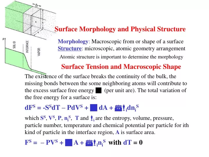
Surface Morphology and Physical Structure. Morphology : Macroscopic from or shape of a surface Structure : microscopic, atomic geometry arrangement. Atomic structure is important to determine the morphology. Surface Tension and Macroscopic Shape.

E N D
Surface Morphology and Physical Structure Morphology: Macroscopic from or shape of a surface Structure: microscopic, atomic geometry arrangement Atomic structure is important to determine the morphology Surface Tension and Macroscopic Shape The existence of the surface breaks the continuity of the bulk, the missing bonds between the some neighboring atoms will contribute to the excess surface free energy g (per unit are). The total variation of the free energy for a surface is: dFS = -SSdT – PdVS + g dA + SmidniS which SS,VS,P, niS, T and mi are the entropy, volume, pressure, particle number, temperature and chemical potential per particle for ith kind of particle in the interface region, A is surface area. FS = – PVS + g A + SminiS with dT = 0
Surface tension Force/length=energy/area g is around half of the energy to melt an atom, since to form surface it needs to break about half bonds of an atom in the cubic. For metal g about 0.16 DHmelting
Wulff construction Liquids and amorphous solids have isotropic g. Therefore they have spherical shape. For crystalline material, g depends on the orientation (hkl) of the surface, while the broken bonds and charge compensation per unit area may be different. g (n) is then the function of orientation of the surface, n. It must have: When we plot g (n) as function of n (Wulff plot), theoretically one can determine the equilibrium shape of a solid. minimum g(hkl) as function of q (the angle between the normal directions of the surface to the {hkl} planes. The Wulff plot gives the shape of the solid (dashed dotted) as the inner envelope of the Wulff planes (broken lines).
Samples of Wulff plot minimum Strong anisotropic case Weakly anisotropic case
How does Wulff plot come? 1 a q cosq na • g(q) can be write as g0cos(q) + g1sin(q)/a g0 is surface tension of (01) plane, g1 is the first order term (proportional to step density) contribution to the surface tension from the existence of the steps. • Therefore g(q) can be shown as 2Rcos(q-Q) = 2R [cosqcosQ + sinqsinQ]. Considering 4 possible quadrants in the plane, a Wulff plot can be shown as in b). With higher order of step density, the plot becomes more complicated as shown before.
Conclusion The Wulff plots consists of a number of circles/spheres, leading to a polygon/polyhedron shape of the crystals, with surfaces of low g preferentially exposed. Any defect effects change vacancy formation energy or mixing defect sites with prefect sites will change g and the plot. g plot will become more spherical when melting T is approached. Crystal growth often occurs under highly non-equilibrium conditions so the equilibrium shape rarely achieved. Surface tension has enormous importance for surface inhomogeneities, such as faceting. Therefore Surface tension plays a important role in the morphology of different crystal surfaces.
Roughening transition Thermal fluctuations is root mean square deviation of the position with respect to the average position. Finite smooth or diverge rough Some cases, rough at any T>0 K (for example 1 dimensional line). Some cases, rough when T>Tr (roughening transition temperature). For example, surface exhibits such a transition at Tr depends on detailed structure. Therefore, for the same element there will be different Tr for different orientation. This implies different g plot at different temperatures too. (See page 15 to 43 of Concepts in Surface Physics ).
Crystal Shape at different temperatures Lead T 323K, crystal is bound by (111), (001), (110) and (112) 323K < T < 393K, (112) facets disappear, (111), (001) and (110) left T > 393K, (110) facets disappear, (111) and (001) left, which are the most closed-packed with highest coordination number of surface atoms
Relaxation, reconstruction, Defects Due to lack of the neighboring atoms for the surface atoms, there are characteristic rearrangement of atoms on the surface. The change of surface structure of semiconductor is more dramatic than metal. Three kinds of this rearrangement can be seen in the shown figure: relaxation, reconstruction and missing row reconstruction.
Relaxation The in-plane lattice same as the bulk with out of-plane one changed. It involves a few layers into the bulk, but often a compensating expansion between the 2nd and 3rd layers can happen with smaller amplitude. The Lower the atomic packing density of the surface, the larger the inward contraction. Low index surfaces of metals (100) and (111) are very close to be simple bulk terminations of the crystal. The more open (110) of almost all metals such as Al(110) usually shows an inward relaxation at the first layer and oscillatory relaxation at next several layers. Almost all nonpolar semiconductor (Si, GaAs…) surfaces show outward expansion of anion and inward contraction of cation: bond rotation theory. Insulator show little relaxation.
The relaxation in metal Cu(410) Tables for relaxation of some clean metal surfaces
The relaxation of wurtzite compounds inward inward outward outward One material called TCC with wurtzite structure
reconstruction Semiconductor’s covalent bonding is strongly directional. For GaAs (110) there is tilt in the surface Ga-As bond of about 27O to the surface and only small change in the bond length.
reconstruction Much more strong reconstruction involves bonds breaking and reforming of new bonds is found in Si(111) surface. All these reconstruction is to lower the total energy at the surface. Although metals rarely have reconstruction, there are some metals like Pt(100) with (2X1) with a missing row of surface atoms and Ir (100) with (5X1) with a buckled quasi-hexagonal layer of surface atoms.
Defects There are also defects like foreign adatoms as interstitials and anti-site exchange of atoms for compound A defect is a break in peridoicity (lattice or basis). Any real crystalline material will contain defects so does the real surface. For the bulk defects in close-packed metals, defects 10-2-10-4 % at room temp.In some alloys (carbides), vacancy defects may approach 50 % at room temp. A well-prepared low-index metal surface contains 0.1-1 % defects. Defects are important to many properties and plays a predominant role in processes such as crystal growth, surface chemical reaction, etc.
fcc(775) Steps Step is one-dimensional or line defects. Steps are very important for the formation of the high-index surfaces formed by small low-index terraces and a high density of steps. Steps often have interesting electronic properties, for example metal steps form the dipole moments.
Review of crystal structure A crystal structure is made up of two basic elements: lattice and basis. The basis can be 1 atom and much more atoms, For example, Si, NaCl have2 atoms basis. There are generally 7 different Crystal Systems. For convenience, these are further divided into 14 Bravais lattices useful information
2-dimensional lattice, Superstructure, and Reciprocal space 5 possible 2-dimensional (2D) Bravais Lattice Centered unit cell can be also be described by a primitive cell. The possible operations for 2D lattice is 1, 2, 3, 4 and 6-fold rotation axes perpendicular to the surface, and mirror planes normal to the surface.
Miller Indices We can define Miller indices (h,k,l) to label crystal planes, which intersects the unit cell at a/h, b/k and c/l. If the plane I cuts an axis at infinity, the corresponding index is zero. There can be also a negative index. Useful links here! In cubic systems only, the [hkl] direction is perpendicular to the (hkl) plane.
Miller Indices for Hexagonal system In the hexagonal system Bravais-Miller Indices may be used by convention (really only need three), including 4 indices (hkil) with h + k = -i. Three symmetry-equivalent axes, 120O apart, and fourth c axis perpendicular to them. i contains no new information and only to identify the structure as hcp.
Surface atom density Fcc 100 110 111
Miller Indices Stepped Surface Characterized by high (hkl) values (Vicinal Surfaces) - (977), (755) or (533). Terrace and step often resemble simple low index planes, therefore there are alternate notation:
Miller Indicesfor Stepped Surface This atom cannot be seen (610) = 6(100) + 1(110) High index steps consists of low index terrace and steps. Useful table
Notations for Superstructures (super lattice) The surface reconstruction will let the surface structure different from the bulk. In many cases, adsorbed layers on a surface will also have different structure. When a different periodicity is present in the topmost atomic layer, this surface lattice is called superlattice and the structure is superstructure. Woods or MatrixNotation is just to tell the relationship between this lattice and the bulk lattice.
Matrix Notation The substrate lattice on the certain surface can be described by a set of 2D translational vectors: rmn= m a1 + n a2(m, n are integers, and a1 and a2 are unit mesh vectors) The adsorbate unit cell is usually defined by the two vectors b1and b2. The relationship between b1and b2can be determined by: b1 = m11a1 + m12a2 b2 = m21a1 + m22a2 m12 or m21 2X2 matrix M detM = | b1 x b2 |/ | a1x a2 | detM is an integer simple superlattice rational number coincidence lattice irrational number incoherent lattice
Woods Notation Wood's notation is the simplest and most frequently used method for describing a surface structure - it only works, however, if the two unit cells are of the same symmetry or closely-related symmetries (more specifically, the angle between b1 & b2 must be the same as that between a1 & a2 ). In essence, Wood's notation first involves specifying the lengths of the two overlayer vectors, b1 & b2 , in terms of a1 & a2 respectively - this is then written in the format : ( |b1|/|a1|x |b2|/|a2| ) In addition, one indicate also the angle through which one mesh is rotated relative to the other. Therefore we can have X{hkl}(pxq) – RO or X{hkl}c(pxq) – RO The possible centering Which substrate surface eg. Si(111)…. p= |b1|/|a1| q= |b2|/|a2| Rotation angle
examples primitive Fcc(100) substrate
examples Substrate : fcc (100)c(2 x 2) overlayer Substrate : fcc (100)(2 x 2) overlayer
2D Reciprocal Lattice For substrate For superstructure or 3 D Reciprocal Lattice
Structural Model of Solid/Solid Interface The important feature of the solid/solid interface is the structure and “abruptness”. The Thermodynamics can give rough idea. Generally the interface is more complicated than the surface. One of the important concept for the film growth is mismatch: difference between the lattice constants of the two materials, usually (b-a)/a with a for substrate and b for the overlayer. The interface depends strongly on both mismatch and thickness.