Download
1 / 17
180 likes | 464 Views
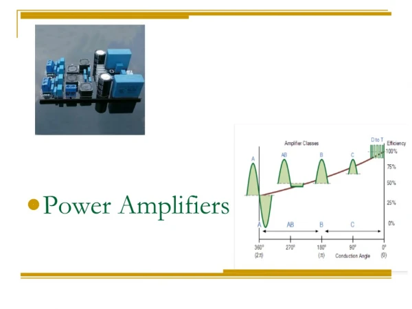
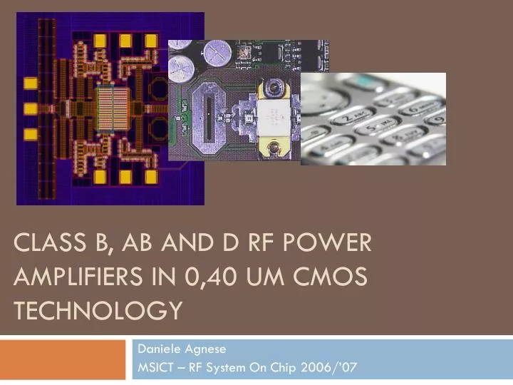
class B, AB and D rf power amplifiers in 0,40 um cmos teChnology. Daniele Agnese MSICT – RF System On Chip 2006/’07. Summary. General idea Technology comparison (CMOS, GaAsFET ) Power amplifiers topology Class B Class AB Class D Project description Simulations/Results Conclusion.

E N D
class B, AB and D rf power amplifiers in 0,40 umcmosteChnology Daniele Agnese MSICT – RF System On Chip 2006/’07
Summary • General idea • Technology comparison (CMOS, GaAsFET) • Power amplifiers topology • Class B • Class AB • Class D • Project description • Simulations/Results • Conclusion
General idea • ADS • Power amplifiers tutorial • Transistor’s model • Circuit adaptation • Simulations change
Technology comparison GaAsFET 0.4 μm CMOS Vth -2.5 V 0.5 V VDS - IDS
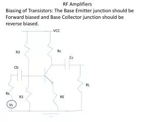
Power amplifier - Class B • Circuit Crossover distortion: 50% of cycle conducting
Power amplifier - Class AB • Circuit
Power amplifier - Class D • Circuit
Project description • Power supply • Working point (Bias ports) • Transistor’s parameters • Power input signal • Load adaptation
Simulations/Results • Class B – 1/2 50% T=1/850 MHz = 1,2 ns Linear region: Vds < Vgs - Vth
Simulations/Results • Class B – 2/2 PAE = (Pload – Pin) / Psupply
Simulations/Results • Class AB – 1/2
Simulations/Results • Class AB – 2/2
Simulations/Results • Class D – 1/2
Simulations/Results • Class D – 2/2
Conclusion • Improvements: • Optimize transistors width • Efficiency • Matching network • Reduce current leakage
Any questions? Doubts? or comments?