Download
1 / 38
380 likes | 505 Views
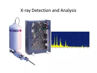
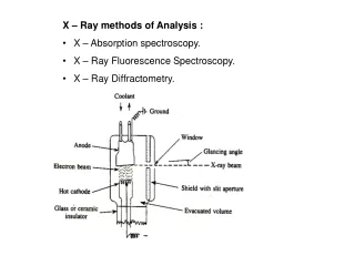
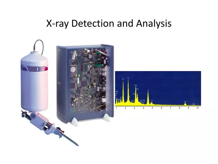
X-ray D etection and Analysis. Principles. K b. K a. When an electron from a K-shell is replaced by one from the second closest shell (M), it is designated as a Kβ event. Certain events such as M α , L β , and K γ are only possible in atoms of sufficient atomic weight.

E N D
Kb Ka When an electron from a K-shell is replaced by one from the second closest shell (M), it is designated as a Kβ event
Certain events such as Mα, Lβ, and Kγ are only possible in atoms of sufficient atomic weight
The Complete Range of Possible Electron Transitions that Give Rise to K, L and M Characteristic X-Rays
# Counts X-ray Energy in KeV An X-ray spectrum for a sample is composed of all the possible signals for that given set of elements. These will differ in terms of energies (KeV) and probabilities (likelihood) scored as number of such signals collected over a given period of time.
Each element has a family of characteristic X-rays associated with it Absorption edge energy: when a photon impinging on an atom carries an energy just above the binding energy of an electron in a specific shell of the atom. The photon can in this case interact with this electron shell and ionize the atom In EDS: we use a much higher energy to excite the electrons to have higher excitation efficiency
In microanalysis we only use the most intense lines, usually the α lines (or, if we can’t resolve them, we use the α and β line). There are energy peak overlaps among different elements, particularly those corresponding to x-rays generated by emission from different energy-level shells (K, L and M) in different elements. For example, there are close overlaps of Mn-Kα and Cr-Kβ, or Ti-Kα and various L lines in Ba. Particularly at higher energies, individual peaks may correspond to several different elements; in this case, the user can apply deconvolution methods to try peak separation, or look at a series of minor peaks if they are present, or simply consider which elements make "most sense" given the known context of the sample.
"Bremsstrahlung" means "braking radiation" and comes from the original German to describe the radiation which is emitted when electrons are decelerated or "braked" when they interact with the specimen. Although they contribute to the total X-ray signal they contain no useful information because their energies are nonspecific and therefore are considered as part of the background .
Bremsstrahlung X-rays are the major part of the continuum X-ray signal that can escape from the deepest portion of the interaction region.
Forensic Applications Bullet fragments (blue) can be identified on cloth fibers and distinguished from other metal pieces by their elemental composition
The proportion of elements present in GSR differ slightly and databases of GSR from different manufacturers can be used to identify what ammunition was used in a crime. GSR is often found on criminals and also on victims if shot at close range.
X-ray mapping Sandstone: K-feldspar (silicon, aluminium, potassium), albite (silicon, aluminium, sodium) and dolomite (calcium, magnesium). The bright blue particles in the silicon map highlight quartz grains.
Pulse Processor Measures the electronic signals to determine the energy of each X-ray detected Analyzer Displays and interprets the X-ray data X-ray Detector Detects and converts X-rays into electronic signals
Cut-away diagram showing the construction of a typical EDS detector. Crystal Collimator FET Window Electron trap
Crystal Collimator FET Window Collimator to limit BSE and stray X-rays Window usually made of beryllium (limited to sodium, atomic number 11) or thin plastic to detect down to boron (Atomic number 5) protects cooled crystal from air.
Crystal Collimator Detector : crystal silicon wafer with lithium added in. For each 3.8 eV from an X-ray, produce an electron and hole. This produces a pulse of current, the voltage of which is proportional to the X-ray energy. Must keep the crystal at LN temperature to keep noise to a minimum. FET : The field effect transistor is positioned just behind the detecting crystal. It is the first stage of the amplification process that measures the charge liberated in the crystal by an incident X-ray and converts it to a voltage output. FET Window
Generation and measurement of electron-hole pairs in the crystal Circuit diagram of the EDS detector (v=Q/C) Typical output voltage “ramp”
The collimating method is unlike the optical lens collimator X-ray without and with a collimator The collimator is made of parallel lead blades
Lithium doped Silicon (SiLi) crystal detector acts as a semiconductor that carries current in a rate proportional to the number of ionization events and acts as an indirect measurement of the energy contained in the X-ray. Li doping to neutralize residual charges produced by impurity in Si The detector (and FET) must be cooled to minimize the current produced by the bias!
Each ionized atom of silicon absorbs 3.8 eV of energy, so an X-ray of 3.8 KeV(e.g. Ca Ka 3.7 KeV) will ionize approximately 1000 silicon atoms. The output voltage is proportional to the X-ray energy. This voltage must be reset (e.g. shining light on the FET) to zero periodically since it can only be increased to a few volts.
One reason that the final lens of an SEM is conical in shape is so that the EDS detector can be positioned at a high take-off angle and inserted close to the specimen for a high solid angle.
Factors affecting signal collection Distance between detector and X-ray source Angle at which detector is struck Volume of signal collected.
Take-off Angle For a given angle of electron incidence, the length of the absorption path is directly proportional to the cosecant (1/sinφ) of the take-off angle, φ
Solid Angle The solid angle Ω of a detector is defined as angle of the cone of signal entering the detector. The greater the size of the detector surface area the greater will be the solid angle.
Larger SiLi crystals will be able to sample a larger volume of signal (better Ω) but because of imperfections in the crystal they have slightly greater noise and thus slightly lower resolution.
Fluorescence Yield (Ratio of x-ray emission to inner-shell ionization)
For a given wavelength λthere is a specific angle θ (Bragg’s angle) at which diffraction will occur. Bragg’s angle is determined by the d-spacing (interplanar spacing) of the crystal and the order of diffraction (n = 1, 2, 3….).
The Bragg angle q and the detector position can be changed by re-positioning the crystal and the detector along a circle called the Rowland circle
A comparison of two spectra collected with EDS and WDS shows how peak overlap and energy spread can serve to obscure the information in an EDS spectrum