Download
1 / 36
360 likes | 373 Views
Vojin G. Oklobdzija, Vladimir M. Stojanovic, Dejan M. Markovic, Nikola M. Nedovic. Digital System Clocking:. Chapter 4: Pipelining and Timing Analysis. High-Performance and Low-Power Aspects. Wiley-Interscience and IEEE Press, January 2003.

E N D
Vojin G. Oklobdzija, Vladimir M. Stojanovic, Dejan M. Markovic, Nikola M. Nedovic Digital System Clocking: Chapter 4: Pipelining and Timing Analysis High-Performance and Low-Power Aspects Wiley-Interscience and IEEE Press, January 2003
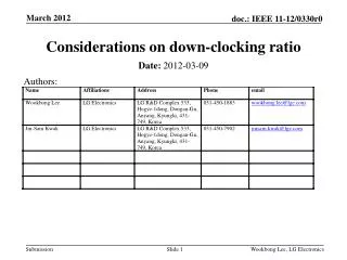
Timing in a digital system using a single clock and flip-flops
Timing in a digital system using a single clock and flip-flops
Late Data Arrival Analysis(single clock, FF) If we set the time reference to t=0 for the leading edge of the clock We set max. clock uncertainties toTL from the nominal time of arrival, TT (for the trailing edge). DCQm represents the minimal Clock-to-Q (output) delay of the Flip-Flop DLm represents minimal delay through the logic (as opposed to index M where DCQM and DLM represent maximal delays).
Late Data Arrival Analysis(single clock, FF) This time ! The latest data arrival in the next cycle is: TL tCR DCQM logic But it should be there at least at this time: U TL So that: Giving us:
Early Data Arrival Analysis(single clock, FF) It is commonly misunderstood that the Flip-Flop provides edge-to-edge timing and is thus easier to use, as compared to the Latch based system, because it does not need to be checked for fast paths in the logic (Hold-time violation). This is not true, and a simple analysis that follows demonstrates that even with the Flip-Flop design the fast paths can represent a hazard and invalidate the system operation.
Early Data Arrival Analysis(single clock, FF) If the clock controlling the Flip-Flop releasing the data is skewed so that it arrives early, and the clock controlling the Flip-Flop that receives this data arrives late, a hazard situation exists. This same hazard situation is present if the data travels through a fast path in the logic. A fast path is the path that contains very few logic blocks, or none at all. This hazard is also referred to as critical race (or race-through)
Early Data Arrival Analysis(single clock, FF) This time ! The earlyest data arrival in the same cycle is: TL DCQm But it should be there not before this time: TL H So that: Giving us limits on the fast paths:
Analysis of a System using a Single Latch System using a single Latch is more complex to analyze than Flip-Flop based one. Single Latch is transparent while the clock in active and the possibility for the race-through exists. This analysis is still much simpler than a general analysis of a system using two Latches (Master-Slave Latch based system). Use of a single Latch represents a hazard due to the transparency of the Latch, which introduces a possibility of races in the system. Therefore, the conditions for the single-latch based system must account for critical race conditions. Presence of the CSE delay decreases the “useful time” in the pipeline cycle. Therefore, in spite of the hazards introduced by such design, the additional performance gain may well be worth the risk.
Late Data Arrival Analysis In the case of a Latch, input signal need to arrive at least a Setup Time U before the trailing edge. This edge could arrive earlier. Thus, the latest arrival of data into the latch that assures reliable capture after the period P has to be: • Data captured at the end of the clock period could be a result of two events (whichever later): • The data was ready, and clock arrived at the latest possible moment TL, and the worse case delay of the Latch i.e. DCQM was incurred. • The clock was active and data arrived at the last possible moment, which is a setup time U and clock skew time TT before the trailing edge of the clock. • In both cases the path through the logic was the longest path DLM. • Under the worse scenario data must arrive in time:
Late Data Arrival Analysis • This gives a constraint for the clock speed in terms of P such as: This inequality breaks down into two inequalities: This shows the minimal bound for Pm, which is the time to traverse the loop: “Starting from the leading edge of a clock pulse, there must be time, under worst case, before the trailing edge of the clock in the next cycle, for a signal to pass through the Latch and the logic block in time to meet the setup time constraint”. The value of P =Pm determines the highest frequency of the clock.
Early Signal Arrival Analysis(Single Latch Based System) The fastest signal, should arrive at the minimum a hold time after the latest possible arrival of the same clock: There are two possible scenarios: (a) signal was latched early and it passed through a fast path in the logic (b) it arrived early while the Latch was transparent and passed through the fast Latch and fast path in the logic. H W after t=0 TT arrived passed Latched early
Early Signal Arrival Analysis(Single Latch Based System) The earliest arrival of the clock tCEL happens when the leading edge of the clock is skewed to arrive at –TL. Thus, the condition for preventing race in the system is expressed as: The earliest possible arrival of the clock, plus clock-to-output delay of the Latch has to occur earlier in time than early arrival of the data, thus: which gives us a lower bound on the signal delay in the logic:
Early Signal Arrival Analysis(Single Latch Based System) The conditions for reliable operation of a system using a single Latch are: the increase of the clock width W may be beneficial for speed, but it increases the minimal bound for the fast paths
Early Signal Arrival Analysis(Single Latch Based System) Maximum useful value for W is obtained when the period P is minimal: Substitute the optimal clock width Wopt we obtain the values for the maximal speed and minimal signal delay in the logic which has to be maintained in order to satisfy the conditions for optimal single-latch system clocking: In a single Latch system, it is possible to make the clock period P as small as the sum of the delays in the signal path: Latch and critical path delay in the logic. This can be achieved by adjusting the clock width W, while taking care of DLmB
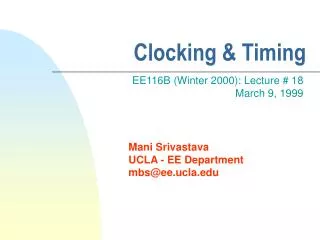
Analysis of a System with two-phase Clock and two Latches in an M-S arrangement
System using two-phase clock and two latches in M-S arrangement
System using two-phase clock and two latches in M-S arrangement From the latest signal arrival analysis, several conditions can be derived. First, we need to assure an orderly transfer into L2 Latch (Slave) from the L1 Latch (Master), even if the signal arrived late (in the last possible moment) into the (Master) L1 Latch. This analysis yields the following conditions: These conditions assure timely arrival of the signal into the L2 Latch, thus an orderly L1-L2 transfer (from Master to Slave)
System using two-phase clock and two latches in M-S arrangement The analysis of the latest arrival of the signal into L1 Latch in the next cycle (critical path analysis) yields to the equations: This conditions assure timely arrival of the signal that starts on the leading edge of f1, traverses the path through L2, the longest path in the logic and arrives before the trailing edge of f1, in time to be captured. The last equation shows that the amount of overlap V between the clocks f 1 and f 2 allows the system to run at greater speed.
System using two-phase clock and two latches in M-S arrangement If we increase V we can tolerate longer “critical path” DLM. However, the increase of the clock introduce a possibility of race conditions, thus requiring a fast path analysis. High-performance systems are designed with the objective of maximizing performance. Therefore, overlapping of the clocks is commonly employed, leading to the constraint of the minimal signal delay in the logic DLmB : The maximal amount of overlap V that can be used is: For maximal performance, it is possible to adjust the clock overlap V so that the system runs at the maximal frequency.
M-S (L1-L2 latch) with non-overlapping clocks F1 and F2 obtained by locally generating clock F2(This arrangement is also commonly referred to as flip-flop)
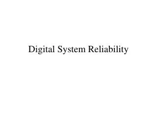
Example:Clocking in the first generation of Alpha Processor(WD21064)
Timing arrangement and Latches used in the first-generation Alpha processor (a) (b)
Example: Clocking the Alpha Processor Clock skew: TL = TT = 20ps, for both edges of the clock. Latch L1 parameters are: clock to Q delay DCQM = 50ps, DCQm= 30ps, D to Q delay DDQM = 60ps, setup time U = 20ps, hold time H = 30ps. Latch L2 parameters are: DCQM = 60ps, DCQm= 40ps, DDQM = 70ps, U = 30ps, H = 40ps. The critical paths in the logic sections 1 and 2 are: DL1M=200pS and DL2M=170ps
Example: Clocking the Alpha Processor For the given clock setup: V=0 and clearly P=W1+W2
Example: Clocking the Alpha Processor Nominal time, t=0 is set at the leading edge of the clock. The latest allowed data arrival times into latches L1 and L2, respectively: The latest arrival time of data into latch L2 is limited by the time at which latch L1 releases the data into the logic stage Logic1: . .
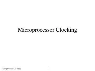
Digital system using a single-phase clock and dual-edge triggered storage elements
Digital system using a single-phase clock and dual-edge triggered storage elements
Allowed clock period as a function of the clock duty cycle in the dual-edge-triggered system