Download
1 / 26
260 likes | 431 Views
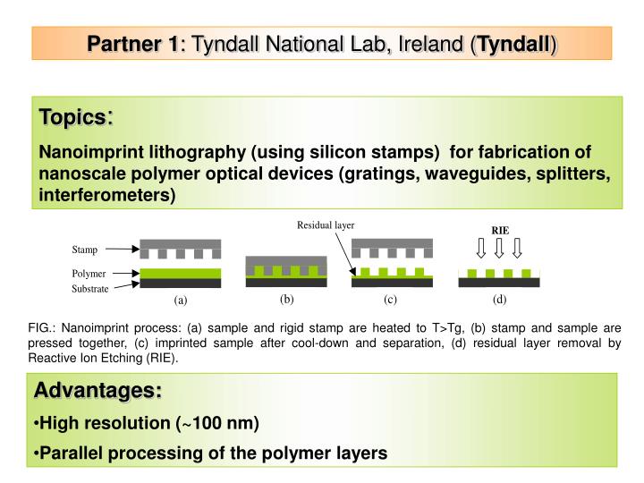
Partner 1 : Tyndall National Lab, Ireland ( Tyndall ). Topics : Nanoimprint lithography (using silicon stamps) for fabrication of nanoscale polymer optical devices (gratings, waveguides, splitters, interferometers).

E N D
Partner 1: Tyndall National Lab, Ireland (Tyndall) Topics: Nanoimprint lithography (using silicon stamps) for fabrication of nanoscale polymer optical devices (gratings, waveguides, splitters, interferometers) FIG.: Nanoimprint process: (a) sample and rigid stamp are heated to T>Tg, (b) stamp and sample are pressed together, (c) imprinted sample after cool-down and separation, (d) residual layer removal by Reactive Ion Etching (RIE). • Advantages: • High resolution (~100 nm) • Parallel processing of the polymer layers
Partner 2: European Lab for Non-linear Spectroscopy (LENS) • Topics: • Random lasers : Explanation of spectra, tuning and switching using liquid crystals (infiltrating the random sample by liquid crystals) • Disorder and order in photonic materials, light transport, Anderson localization of light • Liquid crystals as complex random media (anisotropic multiple light scattering anisotropic diffusion) • Tunable 3D photonic crystals • Development of a controlled single pore infiltration process for re-writeable photonic circuits FIG.: Schematic model of the quasi-two dimensional diffusion process leading to directional and polarized random laser action in a complex system of amplifying liquid crystal droplets in a polymer. Both polarization and threshold of the random laser can be controlled electrically.
Partner 3: ICFO-Institut de Ciències Fotòniques • Topics: • Evanescent wave sensing for safety and biological applications • Tailoring light emission in organic LEDs • Optical manipulation in the nanoscale • Modification of the dispersion of metal nanoparticles through their interaction with a metallic surface – explanation of the effect FIG.:(A-B) 2.4 μm×2.4 μm images recorded simultaneously above the fabricated sample. (A) AFM topography, (B) ASNOM image (illumination from the right). (C-D) Comparison over a unit cell of the theoretical near-field intensity (C) and the experimental data (D).
Partner 4: University of Exeter (UEX) • Topics: • Plasmonics of metallic nanostructures (both localized and extended plasmon modes) • Interaction between molecules and plasmons (including fluorescence and energy transfer) • Plasmons for sensing and imaging (including biosensing and bio-imaging) FIG: Top left – an SEM of silver nanoparticle array fabricated using nanosphere lithography (upper left shows a region where the spheres remain) - light regions are metal, dark the substrate. Top right – an SEM of a square array of particles made using e-beam lithography. Bottom, transmittance spectra of the two samples. The dip in transmittance results from excitation of the localized surface plasmon resonance – note the sharper resonance for the e-beam fabricated sample.
Partner 5: Consejo Superior de Investigaciones Cientificas (CSIC) • Topics: • Preparation and characterization of high quality ZnO/PS composites and ZnO inverted opals of submicron unit cell size, by metalorganic chemical vapor deposition • Band engineering in opals by controlled infiltration with a high index material • Study of the spontaneous emission spectra in 2D photonic crystal microcavities by varying the size and depth of the cavities • Study of the magnetoopical properties of Ni nanowire systems FIG.1: Left (right) panel shows reflectance collected in hexagonal (square) regions of a ZnO inverted opal. Central panel shows the corresponding photonic bands. Fig. 2: Polar Kerr Spectra of Ni nanowires embedded in an alumina matrix for two different nanowires diameters (D) and Kerr rotation spectra of a thick Ni film (for comparison)
Partner 8: Bilkent University (Bilkent) • Topics: • Demonstration of negative EM wave refraction by metallodielectric photonic crystals for a wide incidence angles regime. • Fabrication and characterization of a left-handed material at 100 GHz • Development of optical GaN based quantum modulators • Fabrication and characterization of AlGaN based avalanche photodiodes operating in the solar-blind spectral region FIG.: Electric field intensity at the exit of the metallodielectric photonic crystal. a) for 9 GHz (positive refraction). b) for 9.7 GHz (negative refraction). Incidence angle is 25 degrees.
Partner 10: Koç University (KOÇ) • Topics: • Study of the morphology dependent resonances of silicon microspheres • Demonstration of those resonances using an optical fiber half-coupler and a distributed feedback laser • Demonstration of the ability of the microspheres to be used for filtering applications in optical communication systems FIG.: The experimental setup for the silicon microsphere resonances demonstration (top) and the elastic scattering intensity and power transmission spectra from the microsphere (bottom).
Partner 11: Università di Roma “La Sapienza” (UR-DE) • Topics: • Theoretical analysis of the emission of a dipole pumped by two counter-propagating laser beamsand placedinside a 1D photonic crystal. Demonstration of the emission control through control of the phase difference of the beams • Growth of AlN/GaN films by molecular-organic chemical vapor deposition (MOCVD); demonstration of the non-linear properties of those films (by 2nd harmonic generation measurements) • Development of a set-up for delay time measurements of ps laser pulses FIG.: Top: Lateral section of the investigated AlN/GaN sample. The three layers represent the elementary cell of the DBR structure. Bottom: Second harmonic signal versus the incidence angle, for the AlN/GaN sample. Both fundamental and generated beams are p-polarized. The fundamental beam wavelength is 1064 nm.
Partner 12: Centre National De La Recherche Scientifique (LPN-CNRS) • Topics: • Development of a soft UV assisted nanoimprint lithography (UV-NIL)technique • Application of the UV-NILtechniquefor the fabrication of high aspect ratio nanostructures (resolution ~100 nm, etch depth ~1.5 μm) FIG. 1: Dot array with 200nm diameter before (a) and after (b) lift-off of 20nm thick Nickel • Advantages of the UV-NIL techn.: • Low cost, high flexibility • Simple and fast • Imprinting at ambient temperature and low pressure • Possibility for fine alignment • Good process compatibility for bio applications FIG. 2: SiO2 nano-pillars lattice with 200nm diameter and 1.6 μm depth over a 200×200 μm2
Partner 13: Vilnius Pedagogical University (VPU) • Topics: • Fabrication and characterization of disordered, partially ordered and ordered systems doped with transition metals (TM) and TM compounds • Study of the temperature and field dependence of the properties of the disordered and the partially ordered systems • Study of the band-gap position of the ordered systems as a function of the dopant concentration • Aim: Development of tunable systems FIG. 1: SEM (bar corresponds to 200 nm) micrograph of Fe-doped silica films on Si produced from FeCl3-precursor and annealed in H2 FIG. 2: Reflection spectra of pure (1) and iron-porphyrin (Fe-TPPS)-doped (2,3) silica opal-like structures at angle of incidence equal to 0o (1,2) and 10o (3).
Partner 14: Technical Research Centre of Finland(VTT) • Topics: • Study of a photonic crystal (PC) slab with ring-shaped holes (RPC); demonstration of the increased band gap reflectivity of this PC compared to PCs with air holes • Use of the RPCfor therealization of high-quality cavities (Q~1060) and waveguides of very low group velocities (~0.005c) • Fabrication of opal structures by vertical deposition on to Si templates • Development of a model to estimate the local quality of finite 3D PCs from reflectance spectra FIG. 1: Scanning electron micrograph of a ring photonic crystal patterned into SOI (silicon layer thickness: 240nm). The ring line width is only 70nm FIG. 2:Face-centered cubic (111) opal grown from monodisperse silica spheres with diameter 980 nm by vertical deposition on patterned silicon substrate
Partner 15: Institute of Solid State Physics of the Russian Academy of Sciences(ISSP) • Topics: • ZnO nanocrystals of different shape: • Synthesis by the gas transport method • Measurements of their photoluminescence (PL) spectra under optical excitation • Examination of the PL spectra: mechanisms of generation, mode structure, threshold powers of their UV lasing FIG. 1: Electron-microscope images of the zinc oxide nanorods of different type FIG. 2:PL spectra of the ZnO nanocrystals of the above types at different intensity (kW/cm2) of the exciting nitrogen laser: 1-70, 2-180, 3-600, 4- 2500, 5-8000, 6-22000, 7-33000 and 8- 70000.T=300K.
Partner 16: Universitaet Hamburg(UHamburg) • Topics: • Synthesis of strongly luminescentZnSe, CdTe HgTe and CdHgTe nanocrystals by a wet-chemical based approach • Demonstration of various assembling methods for a controlled preparation of assemblies of semiconductor and/or metal nanocrystals FIG. 1: Typical photoluminescence spectra (normalized) of CdTe, CdHgTe and HgTe nanocrystals. Top right: water soluble emitting powders (ca. 200 mg) of CdTe NCs of 2 different sizes under day light and under UV-lamp excitation. True color image of different solutions of CdTe and ZnSe NCs under UV-lamp excitation. FIG. 2: SEM images of Au/Pt 3D ordered hollow spheres (left) and inverse macroporous opals (right)
Partner 17: Ioffe Physico-Technical Institute of the Russian Academy of Sciences(Ioffe-SP) • Topics: • Study of the nonlinear diffraction and the 2nd harmonic generation enhancement in opal-Si photonic crystals • Study of the modification of the spontaneous emission rate of Er ions placed in 1D photonic crystals (PCs) at the lower photonic band edge • Demonstration of electroluminescent three-dimensional PCs • Demonstration of opal-AgI PCs controlled using the superionic phase transition of AgI • Fabrication of polypyrrole nanowire arrays FIG. 1: Reflection from the (111) surface of the opal-AgI composite: (1) AgI in the semiconductor phase, T=90±C; (2) AgI in the superionic phase, T=150±C. FIG. 2: Intensity of the SH wave reflected from the (111) face of the opal-silicon photonic crystal (filled circles), compared with fundamental radiation reflection spectrum (open circles). Inset: schematic of the “elementary” nonlinear source.
Partner 18: Institute of Molecular and Atomic Physics(IMAPh) • Topics: • Demonstration of brightness enhancement in displays using the anisotropic scattering properties of nanoporous alumina • Demonstration of optically nonlinear ZnSe/ZnS bragg-reflectors. The nonlinearity is due to the resonant electronic interband excitation of ZnSe • Demonstration of strong photoluminescence in CdSe nanocrystals deposited on glass FIG. 1: Angular distribution of scattering from nanoporous alumina for different angles of incident light measured with respect to pore axes. FIG. 2: Microphotoluminescent images of some area of a glass substrate with adsorbed Cd based nanocrystals in the beginning (left) and in the end of the illumination by 488 nm cw lasesr light (6 mW/mm2)
Partner 21: Universite Montpellier 2(UM2) • Topics: • Theoretical and experimental study of the second and third harmonic generation in one-dimensional and two-dimensional GaN photonic crystal (PC) slabs • Demonstration of ~104 enhancement of the second harmonic signal due to the PC; explanation of the effect • Demonstration of photoluminescence in the GaN due to the third harmonic signal FIG. 1: Schematic representation of (a) the 1D PC, (b) the 2D PC excited by the pump radiation. and are the incident and azimuthal angles; k(), k(2), and k(3) denoted the wavevectors of the pump radiation, SH and TH reflected signals, respectively. FIG. 2: Photonic band structure of the 1D PC superimposed on the grey scaled map of the SHG response of the slab. Solid line: the photonic mode dispersion curves at fundamental frequency plotted at twice of their in-plane wave-vectors and frequency. Dotted line: the 5p mode dispersion.
Partner 22: Kungliga Tekniska Hogskolan (KTH) • Topics: • Study of filters with wide range tunability, using one-dimensional photonic crystals (PCs) of Si and SiO2 layers, infiltrated with a liquid crystal (LC) Advantages: Narrower bandwidth compared to conventional waveguides with LC core and SiO2 claddings Top: Cross-section of the directional coupler filter with the “full Bragg Reflection Waveguide (BRW)” arm. Bottom: Cross-section of the filter with the “Liquid Crystal overlay BRW” arm.
Partner 24: Universita degli Studi di Pavia(UPavia) • Topics: • Investigation of single-line defects in Si membranes by angle resolved Reflectance and Attenuated Total Reflectance (ATR) techniques; modeling of the defect-mode dispersion • Phase sensitive measurements on polystyrene artificial opals of different structure parameters • Enhanced third harmonic generation measured in Silicon-On-Insulator (SOI) planar waveguides as well as SOI photonic crystal (PhC) slabs • Simultaneous visible second-harmonic (SH) and ultraviolet third-harmonic (TH) fields generated in a two-dimensional triangular GaN/sapphire photonic crystal FIG: Second harmonic (a) and Third harmonic (b) reflected signals versus azimuth, at 16° incidence, for the GaN photonic crystal (full circles) and for the unpatterned GaN layer (open circles). Insets illustrate the power dependence of the peak signals.
Partner 26: University of Oxford (UOXF.DK) • Topics: • 3D Photonic Crystal device fabrication by holographic lithography combined with scanning two-photon excitation • Fabrication of sub-nm scale photonic devices through binding to DNA self-assembled scaffolds (templates) • Synthesis of 3D periodic DNA nanostructures • Formation of chiral DNA nanotubes (<100 nm diameter, ~1 μm length), candidates for optical wires based on near-field interactions • Synthesis of molecular motors able to move along DNA tracks (to be exploited in the fabrication of self-organized molecular devices)
Partner 27: Institutul National De Cercetare Dezvoltare Pentru Fizica Laserilor, Plasmei Si Radiatiei(NILPRP) • Topics: • Study of spatial solitons in one-dimensional waveguide arrays with cubic nonlinearities; waveguidearrays are generated by fs laser pulses • Investigation of Planck spectra of spherical microcavities; discrete Planckspectra are calculated for small cavities • Study of the effects of χ(3)nonlinearities in various structures FIG. 1: Dynamics of Soliton Wave guides induced with fs laser beam in lithium niobate crystals FIG. 2: The beam profile at the output face of the crystal, for free (left) and guided (right) propagation through the lithium niobate crystal
Partner 29: Ecole Normale Superieure Cachan(ENS-Cachan) Topics: Nanoimprint lithography (using silicon stamps) for fabrication of nanoscale polymer optical devices (gratings, waveguides, splitters, interferometers) FIG.: Nanoimprint process: (a) sample and rigid stamp are heated to T>Tg, (b) stamp and sample are pressed together, (c) imprinted sample after cool-down and separation, (d) residual layer removal by Reactive Ion Etching (RIE). • Advantages: • High resolution (100 nm?) • Parallel processing of the polymer layers
Partner 30: The Queen's University of Belfast(QUB) • Topics: • Development of high resolution techniques for the characterization of micromagnetic and magnetooptical properties of materials (like near field microscopy of 2nd harmonic generation) • Studies of various types of linear and nonlinear surface plasmon polariton crystals (fabrication & characterization) • Device of a procedure for the creation of self-organized templates used for the formation of nanostructures; formation of ferromagnetic and metallic nanostructures • Study of the magnetooptical properties of nanostructured metal films • Theoretical study of the quantum nature of light-molecule interactions (for quantum computing applications FIG. 1: Topography (left) and the polarisation-dependent SHG variations from the PZT thin film. FIG. 2: The Au nanowire array achieved after removing the alumina template.
Partner 32: Foundation for Research and Technology - Hellas(FORTH) • Topics: • Theoretical and experimental study of the emission from a narrow photonic crystal (PC) waveguide; demonstration of highly directional emission for proper PC terminations • Study of the emission rate of dipoles in PC membranes; examination of the dependence of the emission rate on the frequency and the position of the dipole • Study of micrometer scale metamaterials with negativeeffective permeability (μ) in the THz range; examination of the frequency limitations of this negative μ • Study of the negative refraction and the focusing properties of photonic crystals FIG. 1: Intensity distribution of light exiting a 2D photoniccrystal waveguide for two different structure terminations. FIG. 2: The magnetic field of a Gaussian beam undergoing reflection and refraction at the surface of a PC in the negative refraction regime
Partner 33: Stichting voor Fundamenteel Onderzoek der Materie(FOM) • Topics: • Development of an angle-resolved transmission/reflection setup for investigation of micrometer scale photonic samples • Development of a phase-sensitive, time-resolved near-field optical microscope • Study of transmission through periodic arrays of subwavelength holes in metallic films; extraordinary transmission was found; resonances of the individual holes play and important role • Experimental detemination of the band structure in photonic crystal waveguides; observation of ultraslow light in such guides FIG. 1: The normalized transmission for y-polarized light of periodic arrays of holes in metallic films, for different aspect ratio of the holes (hole area is constant). The legends show the aspect ratios of the holes. In the insets the used axes are displayed. FIG. 2: Schematic representation of a pulse tracking experiment on a photonic crystal waveguide
Partner 34: Consorzio Ricerche Elaborazione Commutazione Ottica Milano(CORECOM) • Topics: • Characterization of active optical planar waveguide devices • Theoretical analysis of non-linear optical propagation in slow wave structures made of coupled resonators • Characterization of Er-doped polymeric waveguide amplifiers • Production and characterization of ordered nanostructured porous aluminum oxide FIG. 1: Examples of direct-coupled optical resonator slow wave structures (SWS); (a): direct coupled Fabry-Perot; (b): SWS direct coupled microring SWS; (c): PBG-SWS. FIG. 2: Samples of anodic aluminium porous oxide obtained in phosphoric acid. (a): partial ordering by two-steps anodization of an aluminium foil 99,995%; (b): hexagonal 2D lattice, obtained by pre-patterning of the aluminium foil, using 60°-rotated gratings as molds;
Partner 35: Bergische Universitatet Wuppertal(BUW) • Topics: • Synthesis of dye-coated semiconducting polymer nanoparticles • Study of excitation energy transfer from semiconducting polymer nanoparticles to surface-bound fluorescent dyes FIG. 1: Absorption (solid line) and emission (dashed line) spectra of PF2/6 nanoparticle dispersion and of Rhodamine 6G. FIG. 2: Emission spectra of PF2/6 nanoparticle dispersions (dotted curves) and of Rhodamine 6G-coated nanoparticle dispersions with λex of 374 nm. The inset shows the emission spectra (dashed curves) of dye-coated nanoparticles excited at 527 nm into the absorption band of the dye (wavelength region 550-700 nm).