Download
1 / 4
40 likes | 137 Views
3D silicon sensors at beam-lines. Cinzia Da Via, The University of Manchester UK, Daniela Bortoletto , Oxford University, UK GianFranco Dalla Betta , INFN and Trento University , Italy.

E N D
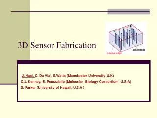
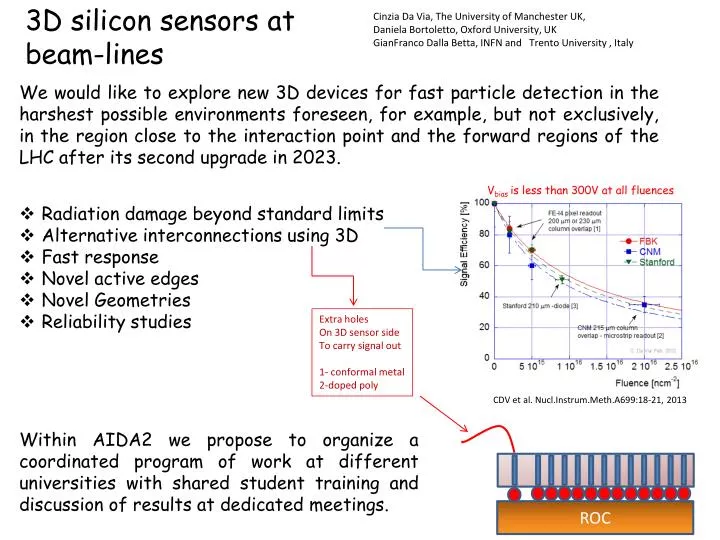
3D silicon sensors at beam-lines Cinzia Da Via, The University of Manchester UK, Daniela Bortoletto, Oxford University, UK GianFrancoDallaBetta, INFN and Trento University , Italy We would like to explore new 3D devices forfast particle detection inthe harshest possible environments foreseen, for example, but not exclusively, in the region close to the interaction point and the forward regions of the LHC after its second upgrade in 2023. • Radiation damage beyond standard limits • Alternative interconnections using 3D • Fast response • Novel active edges • Novel Geometries • Reliability studies Vbiasis less than 300V at all fluences Extra holes On 3D sensor side To carry signal out 1- conformal metal 2-doped poly CDV et al. Nucl.Instrum.Meth.A699:18-21, 2013 Within AIDA2 we propose to organizea coordinated program of work at different universitieswith shared student training and discussion of results at dedicated meetings. ROC
Example1: fast Responses using thin 3D with charge multiplication by design Sentaurus simulation package M. Povoli and G-F DallaBetta (University of Trento, Italy) Size = 10 x 10 x 1mm3 Column radius = 2mm Electrode doping = 5x1019cm-3 Bulk doping = 1x1013cm-3 Transients with minimum-ionizing particles (5.9) (5.5) 60ps Electric Field distribution V=130V Time (s) Electric potential distribution GAIN at3 different positions
Example2: Alternative active edge design in double-side 3D S. Parker (2012) Doping Concentration [cm-3] A p+ doped wall exploiting diffusion from small trenches … Sentaurus simulation package M. Povoli and G-F DallaBetta (University of Trento, Italy)
Milestones, Deliverables and Funds Milestone1 Definition and simulation of novel layouts with enhanced speed, radiation tolerance and novel active edges for upgrades of theLHC experiments and novel applications Deliverable1: novel test structures design and processing Milestone2 Integration of test structures with existing readout electronics chips Deliverable2: Laboratory and Beam tests before and after irradiation Milestone3 Analysis and comparison with existing data Deliverable3: Presentation of novel data at meetings and conferences Funds: Requested funds would support PhD students at the Universities of Trento, Manchester and Oxford to carry out laboratory and beam tests of fabricated novel 3D structures. Funds would also be requested for student exchange, travelat beamtests and attendance to schools and conferences during a period of 3 years. Contacts are existing with FBK, Trento, I, CNM Barcelona, S, and SINTEF Oslo, N