Download
1 / 36
370 likes | 949 Views
마이크로프로그램된 제어 (Microprogrammed Control). Lecture #7. 강의 목차. Control Unit Control Memory Sequencing Microinstructions Microprogram Example Design of Control Unit Nanostorage and Nanoprogram. 제어 장치 (1). 제어 장치 (Control Unit) 명령어 실행을 위해 요구되는 마이크로 연산들을 연속적으로 수행하는 제어 신호를 보냄으로써 명령어 실행을 제어

E N D
마이크로프로그램된 제어(Microprogrammed Control) Lecture #7
강의 목차 • Control Unit • Control Memory • Sequencing Microinstructions • Microprogram Example • Design of Control Unit • Nanostorage and Nanoprogram 컴퓨터시스템구조
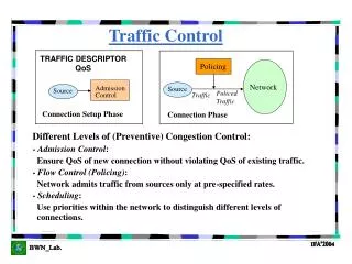
제어 장치 (1) • 제어 장치(Control Unit) • 명령어 실행을 위해 요구되는 마이크로 연산들을 연속적으로 수행하는 제어 신호를 보냄으로써 명령어 실행을 제어 • Control signal(that specify microoperations) in a bus-organized system • groups of bits that select the paths in multiplexers, decoders, and arithmetic logic units • 제어 장치 구현 방식 • Hardwired Control • Microprogrammed Control 컴퓨터시스템구조
Control Data Memory I R Status F/Fs Control Unit's State Timing State Control Combinational CPU Points Logic Circuits Ins. Cycle State 제어 장치 (2) • 제어 장치 구현 방식 (계속) • Hardwired Control : 5장 참조 • 제어 논리가 게이트, 플립플롭, 디코더 그리고 다른 논리 장치를 이용하여 구현 • 장점: 빠른 처리 속도, 단점: 설계 변경 시에 회로 변경 컴퓨터시스템구조
M Control Data e m Status F/Fs o I R r y Control C C C Next Address Storage S S D P CPU Generation (-program A D s Logic } R R memory) 제어 장치 (3) • 제어 장치 구현 방식 (계속) • Microprogrammed Control • 제어 정보를 제어 메모리에 저장하고, 제어 메모리에 프로그램된 제어 정보를 이용하여 원하는 일련의 마이크로 연산을 실행 • 장점: 제어 메모리에 저장된 마이크로 프로그램을 수정하여 기능 변경 • 단점: 늦은 처리 속도 컴퓨터시스템구조
Microprogrammed Control Unit(1) • 제어 워드(Control Word) • 버스 구조의 시스템에서 멀티플렉서, 디코더 등의 정보 전달 선택 및 산술논리연산장치의 역할 등을 결정하는 비트의 모임이 어떤 마이크로 연산을 수행할 것인지 결정 • 이러한 일련의 비트 모임을 ‘제어 워드’라 하며, 특수한 제어 메모리에 저장 • 마이크로 명령어(Microinstruction) • 하나 이상의 마이크로 연산을 정의 • 제어 워드(Control Word)와 시퀀싱 워드(Sequencing Word)로 구성 • 제어 워드 - All the control information required for one clock cycle • 시퀀싱 워드 - Information needed to decide the next microinstruction address • 마이크로 프로그램(microprogram)을 작성하는 단위(Vocabulary) 컴퓨터시스템구조
Microprogrammed Control Unit(2) • 마이크로 프로그램(Microprogram) • 하나의 기계어 명령어 집합을 정상적으로 실행하기 위해 요구되는 모든 제어 신호를 생성하기 위해 제어 메모리에 저장된 프로그램 • 마이크로 명령어로 구성 • 제어 메모리(Control Memory or Control Storage) • 마이크로프로그램된 제어 장치에서 마이크로 프로그램을 저장하는 저장 장치 • 초창기에는 read-only 메모리를 사용 Static Microprogramming • Writeable Control Memory(Writeable Control Storage:WCS) • 내용을 수정할(writable) 수 있는 제어 메모리 -> Allows the microprogram can be changed -> Instruction set can be changed or modified 컴퓨터시스템구조
Microprogrammed Control Unit(3) • 동적 마이크로 프로그래밍(Dynamic Microprogramming) • Computer system whose control unit is implemented with a microprogram in WCS • Microprogram can be changed by a systems programmer or a user • 마이크로 명령어 실행 컴퓨터시스템구조
Microprogrammed Control Unit(4) • 마이크로프로그램된 제어 장치 구성 1) 제어 메모리(Control Memory) • Microprogram을 저장 • Computer Memory(employs a microprogrammed control unit) • Main Memory : for storing user program (Machine instruction/data) • Control Memory : for storing microprogram (Microinstruction) 2) 제어 주소 레지스터(Control Address Register) • 제어 메모리로부터 읽어올 마이크로 명령어 주소를 지정 컴퓨터시스템구조
Microprogrammed Control Unit(5) • 마이크로프로그램된 제어 장치 구성 3) 시퀀서(Sequencer = Next Address Generator) • 제어 메모리로부터 제어 명령어를 읽어올 주소 시퀀스를 생성 • 다음 마이크로 명령어의 주소는 입력에 따라 여러 가지 방법으로 결정 4) 제어 데이터 레지스터(Control Data Register = Pipeline Register) • 제어 메모리에서 읽어 온 마이크로 명령어를 저장 • 매 클럭 펄스마다 데이터 레지스터의 제어 워드에서 지정하는 마이크로 연산과 다음 마이크로 명령어를 읽어오는 동작을 동시에 수행 컴퓨터시스템구조
주소 시퀀싱 (1) • 주소 시퀀싱(Address Sequencing) • Sequencer(Next Address Generator) • 제어 메모리에 대한 일련의 접근 주소를 생성 • 루틴(Routine) • 제어 메모리에 저장된 마이크로 명령어 그룹 • 각 기계어 명령어는 명령어를 수행하는 루틴을 갖는다 • 맵핑(Mapping) • Instruction Code Address in control memory(where routine is located) • 제어 메모리 접근 주소 결정 방법 1) 제어 주소 레지스터를 하나 증가 2) 무조건 분기와 상태 비트 조건에 따른 조건부 분기 3) 명령어 비트(Op-code)들로부터 제어 메모리 주소 맵핑 4) 서브루틴을 호출하고 복귀하는 기능 컴퓨터시스템구조
주소 시퀀싱 (2) • 제어 메모리의 주소 생성 하드웨어: Fig. 7-2 • Multiplexer • CAR Increment • JMP/CALL • Mapping • Subroutine Return • CAR : Control Address Register • CAR receive the address from 4 different paths 1) Incrementer 2) Branch address from control memory 3) Mapping Logic 4) SBR : Subroutine Register • SBR : Subroutine Register • Return Address can not be stored in ROM • Return Address for a subroutine is stored in SBR 컴퓨터시스템구조
주소 시퀀싱 (3) • 제어 메모리의 주소 생성 하드웨어 (계속) • 조건부 분기(Conditional Branching) • Status Bits • 분기 논리(Brach Logic)에서의 선택적인 분기 동작을 제어 • Branch Logic • 특정 상태를 테스트하고 조건에 맞다면 주어진 주소로 분기하고, 그렇지 않다면 바로 다음의 마이크로 명령어를 수행하도록 설정(increment) • Status Bit Test와 Branch Logic의 실제회로: Fig. 7-8 • 4 X 1 Mux 와 Input Logic(Tab. 7-4)으로 구성 Load address Control address register Increment MUX Control memory ... Status (condition) bits Micro-operations Condition select 컴퓨터시스템구조
주소 시퀀싱 (4) • 제어 메모리의 주소 생성 하드웨어 (계속) • 무조건부 분기(Unconditional Branching) • 제어 메모리로부터 분기 주소를 적재함으로써 구현 • 상태 비트(status bit) 중에 하나를 항상 1로 고정하고 이 상태 비트를 선택함 컴퓨터시스템구조
주소 시퀀싱 (5) • 제어 메모리의 주소 생성 하드웨어 (계속) • 명령어 맵핑(Mapping of Instruction) : Fig. 7-3 • 4 bit Opcode = specify up to 16 distinct instruction • Mapping Process : Converts the 4-bit Opcode to a 7-bit control memory address • 1) Place a “0”in the most significant bit of the address • 2) Transfer 4-bit Operation code bits • 3) Clear the two least significant bits of the CAR (즉, 4 개의 Microinstruction 수용가능) • Mapping Function : Implemented by Mapping ROM or PLD • Control Memory Size : 128 words (= 27) 컴퓨터시스템구조
주소 시퀀싱 (6) Direct Mapping Address • 제어 메모리의 주소 생성 하드웨어 (계속) • 명령어 맵핑(Mapping of Instruction) (계속) 0000 0001 0010 0011 0100 OP-codes of Instructions ADD Routine AND Routine ADD AND LDA STA BUN 0000 0001 0010 0011 0100 LDA Routine . . . STA Routine BUN Routine Control Storage Mapping Bits 10 xxxx 010 Address ADD Routine 10 0000 010 AND Routine 10 0001 010 10 0010 010 LDA Routine 10 0011 010 STA Routine 10 0100 010 BUN Routine 컴퓨터시스템구조
주소 시퀀싱 (7) • 제어 메모리의 주소 생성 하드웨어 (계속) • 명령어 맵핑(Mapping of Instruction) (계속) OP-code Machine Instruction : 1 0 1 1 Address Mapping bits : 0 x x x x 0 0 0 1 0 1 1 0 0 Microinstruction address : Mapping function implemented by ROM or PLA : OP-code Mapping memory (ROM or PLA) Control address register Control Memory 컴퓨터시스템구조
주소 시퀀싱 (8) • 제어 메모리의 주소 생성 하드웨어 (계속) • 서브루틴(Subroutine) • 다른 루틴에서 사용되는 프로그램 모듈 마이크로 프로그램 안에서 어디에서도 호출 가능 • 동일한 마이크로 코드 모임을 서브루틴화함으로써 제어 메모리를 절약 가능 • 예제) Memory Reference 명령에서Operand의Effective Address를 구하는Subroutine • 표. 7-2에서 INDRCT(여기에서 FETCH와 INDRCT는 Subroutine) • Subroutine은 ORG 64, 즉 1000000 -1111111에 위치(Routine은0000000 -0111111) • 서브루틴 호출과 반환 • 서브루틴 호출 동안에 반환 주소를 저장 • 서브루틴 반환 시에 반환 주소를 재저장(복원) • Last-In First Out(LIFO) Register Stack 컴퓨터시스템구조
마이크로 프로그램 예제 (1) • 컴퓨터 하드웨 구성: Fig. 7-4 • 2개의 Memory • Main memory(instruction/data) • Control memory(microprogram) • Data written to memory come from DR, and Data read from memory can go only to DR • 4 CPU Registers and ALU : • DR, AR, PC, AC, ALU • DR can receive information from AC, PC, or Memory (selected by MUX) • AR can receive information from PC or DR (selected by MUX) • PC can receive information only from AR • ALU performs microoperation with data from AC and DR (결과는AC에 저장) • 2 Control Unit Register : SBR, CAR 컴퓨터시스템구조
마이크로 프로그램 예제 (2) • 명령어 형식(Instruction Format) • Instruction Format : Fig. 7-5(a) • I : 1 bit for indirect addressing • Opcode : 4 bit operation code • Address : 11 bit address for system memory • Machine Instruction : Fig. 7-5(b) • 16 명령어가 가능하며 4개만 표시 0 15 14 11 10 Opcode I Address Symbol OP-code Description • ADD 0000 AC AC + M[EA] • BRANCH 0001 if (AC < 0) then (PC EA) • STORE 0010 M[EA] AC • EXCHANGE 0011 AC M[EA], M[EA] AC EA is the effective address 컴퓨터시스템구조
3 3 3 2 2 7 F1 F2 F3 CD BR AD F1, F2, F3: Microoperation fields CD: Condition for branching BR: Branch field AD: Address field 마이크로 프로그램 예제 (3) • 마이크로 명령어 형식(Microinstruction Format) : Fig. 7-6 • 3 bit Microoperation Fields : F1, F2, F3 • 총 21개 Microoperation : Tab. 7-1 • 동시에 3 개의 microoperation 실행가능 • 3 개 이하일 경우, 000(no operation)으로 채움 • 두 개 또는 그 이상의 충돌하는 마이크로 연산은 동시에 설정할 수 없음. • 예제) 010 001 000 AC를 0으로 클리어하는 동시에 AC에서 DR를 빼는 동시에 수행하여 충돌 발생 • 기호DRTAC(F1 = 100) • DR에서 AC로의 레지스터 전송을 다섯 개의 문자로 표현(T = to) 컴퓨터시스템구조
마이크로 프로그램 예제 (4) • 마이크로 명령어 형식(Microinstruction Format) (계속) • 2 bit Condition Fields : CD • 00 : Unconditional branch, U = 항상 1 • 01 : Indirect address bit, I = DR(15) • 10 : Sign bit of AC, S= AC(15) • 11 : Zero value in AC, Z = AC = 0 • 2 bit Branch Fields : BR • 00 : JMP • Condition = 0 : 1 CAR ← CAR+1 • Condition = 1 : 2 CAR ← AD • 01 : CALL • Condition = 0 : 1 CAR ← CAR+1 • Condition = 1 : 2 CAR ← AD, SBR ← CAR+1 • 10 : RET3 CAR ← SBR • 11 : MAP4 CAR(2-5) ← DR(11-14), CAR(0,1,6) ← 0 • 7 bit Address Fields : AD • 128 word : 128 X 20 bit 컴퓨터시스템구조
마이크로 프로그램 예제 (5) • 마이크로 명령어 형식(Microinstruction Format) : Tab. 7-1 F1 Microoperation Symbol 000 None NOP 001 AC ← AC + DR ADD 010 AC ← 0 CLRAC 011 AC ← AC + 1 INCAC 100 AC ← DR DRTAC 101 AR ← DR(0-10) DRTAR 110 AR ← PC PCTAR 111 M[AR] ← DR WRITE F2 Microoperation Symbol 000 None NOP 001 AC ← AC - DR SUB 010 AC ← AC ∨ DR OR 011 AC ← AC ∧ DR AND 100 DR ← M[AR] READ 101 DR ← AC ACTDR 110 DR ← DR + 1 INCDR 111 DR(0-10) ← PC PCTDR F3 Microoperation Symbol 000 None NOP 001 AC ← AC DR XOR 010 AC ← AC’ COM 011 AC ← shl AC SHL 100 AC ← shr AC SHR 101 PC ← PC + 1 INCPC 110 PC ← AR ARTPC 111 Reserved • BR Symbol Function • 00 JMP CAR AD if condition = 1 • CAR CAR + 1 if condition = 0 • 01 CALL CAR AD, SBR CAR + 1 if condition = 1 • CAR CAR + 1 if condition = 0 • 10 RET CAR SBR (Return from subroutine) • 11 MAP CAR(2-5) DR(11-14), CAR(0,1,6) 0 CD Condition Symbol Comments 00 Always = 1 U Unconditional branch 01 DR(15) I Indirect address bit 10 AC(15) S Sign bit of AC 11 AC = 0 Z Zero value in AC ○ + 컴퓨터시스템구조
마이크로 프로그램 예제 (6) • 기호로 표시된 마이크로 명령어(Symbolic Micoinstruction) • ① Label Field : Terminated with a colon ( : ) • ② Microoperation Field : one, two, or three symbols, separated by commas • ③ CD Field : U, I, S, or Z • ④ BR Field : JMP, CALL, RET, or MAP • ⑤ AD Field • a. Symbolic Address : Label ( = Address ) • b. Symbol “NEXT”: next address • c. Symbol “RET”or “MAP”: AD field = 0000000 • ORG : Pseudoinstruction(define the origin, or first address of routine) 컴퓨터시스템구조
마이크로 프로그램 예제 (7) • Fetch 루틴 • Memory Map(128 words) : Tab. 7-2, Tab. 7-3 • Address 0 to 63 : Routines for the 16 instruction(현재는 4 instruction) • Address 64 to 127 : Any other purpose(현재는Subroutines : FETCH, INDRCT) • FETCH 서브루틴의 마이크로 명령어 • Fetch 서브루틴 : 주소 64에서 시작 컴퓨터시스템구조
마이크로 프로그램 예제 (8) • Fetch 루틴 (계속) • 어셈블러에 의해 변환된 이진 마이크로 명령어 Binary address F1 F2 F3 CD BR AD 1000000 110 000 000 00 00 1000001 1000001 000 100 101 00 00 1000010 1000010 101 000 000 00 11 0000000 컴퓨터시스템구조
마이크로 프로그램 예제 (9) • 기호화된 마이크로 프로그램(Symbolic Microprogram) • 표 7.2 : Fetch 루틴, Indirect 서브루틴, ADD, BRANCH, STORE 루틴 • FETCH 서브루틴에서 MAP 마이크로 명령어 실행 • Branch to address 0xxxx00 (xxxx = 4 bit Opcode) • ADD : 0 000000 = 0 • BRANCH : 0 000100 = 4 • STORE : 0 001000 = 8 • EXCHANGE : 0 001100 = 12, ( 16, 20, …, 60) • INDRCT 서브루틴 • 기계 명령어 실행 루틴에 간접 주소 모드(Indirect Address : I= 1)인 경우 호출 • Indirect Addressing : • AR이 지시하는 메모리 내용을 DR에 읽은 후, 다시 AR에 써넣는다 컴퓨터시스템구조
마이크로 프로그램 예제 (10) • 기호화된 마이크로 프로그램(Symbolic Microprogram) : Tab. 7-2 Label Microops CD BR AD ADD: BRANCH: OVER: STORE: EXCHANGE: FETCH: INDRCT: ORG 0 NOP READ ADD ORG 4 NOP NOP NOP ARTPC ORG 8 NOP ACTDR WRITE ORG 12 NOP READ ACTDR, DRTAC WRITE ORG 64 PCTAR READ, INCPC DRTAR READ DRTAR I U U S U I U I U U I U U U U U U U U CALL JMP JMP JMP JMP CALL JMP CALL JMP JMP CALL JMP JMP JMP JMP JMP MAP JMP RET INDRCT NEXT FETCH OVER FETCH INDRCT FETCH INDRCT NEXT FETCH INDRCT NEXT NEXT FETCH NEXT NEXT NEXT 컴퓨터시스템구조
마이크로 프로그램 예제 (11) • 기호화된 마이크로 프로그램(Symbolic Microprogram) • ADD instruction 실행절차 1) ADD 명령이 실행되면 FETCH subroutine에서 Opcode를 fetch한 후, MAP이 실행되면 MAP Process에 의해 CAR = 0000000으로 branch 한다(여기서 Opcode = 0000, Fig. 7-5(b)) 2) ADD 명령의 Address 0에서는CD 비트를 검사하여 Indirect = 1이면 INDRCT subroutine에서 Effective Address를 AR에 써넣고 반환된다. 3) ADD 명령의 Address 1 에서는 AR이 지시하는 Memory의 내용을 읽어서 DR에 써넣는다. 4) ADD 명령의 Address 2 에서는AC + DR을 AC에 저장한 후, FETCH subroutine으로 Branch하면 1)에서와 같은 방법으로 PC가 지시하는 명령어를 Fetch하여 MAP 수행 결과에 따라 해당 Routine Address로 Branch 한다. • BRANCH instruction 실행절차 1) BRANCH 명령의 Address 4 에서는CD Bit를 검사하여 Sign(S) = 1이면 Address 6번으로 가서 Indirect를 검사하고 ARTPC에 의해 해당 Address로 Branch한 후, FETCH에 의해 PC가 지시하는 다음 명령을수행한다. 2) BRANCH 명령의 Address 4에서 Sign = 0이면 Branch하지 않고 FETCH에 의해PC가 지시하는 다음 명령을 수행한다. 컴퓨터시스템구조
마이크로 프로그램 예제 (12) • 이진 마이크로 프로그램(Binary Microprogram) : Tab. 7-3 • 기호화된 마이크로 프로그램은 어셈블러나 사람에 의해 직접 이진 코드로 변환되어야 제어 메모리에 적재할 수 있다 • 표. 7-3의 3번지의 코드는 사용되지 않는 워드이기 때문에 모든 코드가 0으로 채워져 있지만 CAR 값이 잡음 등으로 3번지로 설정되는 경우를 고려하여 fetch 루틴으로 brach하게 설정됨. • ROM 기반 제어 메모리(Control Memory) • Most microprogrammed systems use a ROM for the control memory • Cheaper and faster than a RAM • Prevent the occasional user from changing the architecture of the system 컴퓨터시스템구조
마이크로 프로그램 예제 (13) • 이진 마이크로 프로그램(Binary Microprogram): Tab. 7-3 • Address Binary Microinstruction • Micro Routine Decimal Binary F1 F2 F3 CD BR AD • ADD 0 0000000 000 000 000 01 01 1000011 • 1 0000001 000 100 000 00 00 0000010 • 2 0000010 001 000 000 00 00 1000000 • 3 0000011 000 000 000 00 00 1000000 • BRANCH 4 0000100 000 000 000 10 00 0000110 • 5 0000101 000 000 000 00 00 1000000 • 6 0000110 000 000 000 01 01 1000011 • 7 0000111 000 000 110 00 00 1000000 • STORE 8 0001000 000 000 000 01 01 1000011 • 9 0001001 000 101 000 00 00 0001010 • 10 0001010 111 000 000 00 00 1000000 • 11 0001011 000 000 000 00 00 1000000 • EXCHANGE 12 0001100 000 000 000 01 01 1000011 • 13 0001101 001 000 000 00 00 0001110 • 14 0001110 100 101 000 00 00 0001111 • 15 0001111 111 000 000 00 00 1000000 • FETCH 64 1000000 110 000 000 00 00 1000001 • 65 1000001 000 100 101 00 00 1000010 • 66 1000010 101 000 000 00 11 0000000 • INDRCT 67 1000011 000 100 000 00 00 1000100 • 68 1000100 101 000 000 00 10 0000000 컴퓨터시스템구조
제어 장치의 설계 (1) • 마이크로 명령어 필드의 디코딩 : Fig. 7-7 • 3x8 디코더를 사용하여 마이크로 명령어의 제어 워드 F1, F2, F3를 디코딩 • 디코더 출력 신호는 해당 마이크로 연산을 실행 초기화시키는 장치에 연결된다 • 예제) F1 = 101 (5) : DRTAR F1 = 110 (6) : PCTAR • Output 5 and 6 of decoder F1 are connected to the load input of AR (two input of OR gate) • Multiplexer select the data from DR when output 5 is active • Multiplexer select the data from AC when output 5 is inactive 컴퓨터시스템구조
제어 장치의 설계 (2) • 마이크로 명령어 필드의 디코딩 : Fig. 7-7 • Arithmetic Logic Shift Unit • Control signal of ALU in hardwired control: p. 164, Fig. 5-19, 20 • Control signal will be now come from the output of the decoders associated with the AND, ADD, and DRTAC. 컴퓨터시스템구조
제어 장치의 설계 (3) • Microprogram Sequencer: Fig. 7-8 • 제어 메모리의 다음 접근 주소를 결정 • MUX 1 • Select an address source and route to CAR ① CAR + 1 ② JMP/CALL ③ Mapping ④ Subroutine Return • JMP와 CALL의 차이점 • JMP : AD가 MUX 1의 2번을 통해 CAR로 전송 • CALL : AD가 MUX 1의 2번을 통해 CAR로 전송되고, 동시에 CAR + 1(Return Address)이 LOAD 신호에 의해 SBR에 저장된다. S1S0 Address Source 00 CAR + 1, In-Line 01 SBR RETURN 10 CS(AD), Branch or CALL 11 MAP 컴퓨터시스템구조
1 L L(load SBR with PC) for subroutine Call From CPU Test I MUX2 T S Input BR field of CS Z Select I0 S0 S1 for next address selection logic I1 CD Field of CS 제어 장치의 설계 (4) • Microprogram Sequencer: Fig. 7-8 • MUX 2 • 상태 비트를 검사하고 검사 결과를 입력 논리 회로에 적용 • Condition bit(CD)에 근거하여 4개의 상태 비트 중에 하나를 선택 • 입력 논리 회로(Input Logic Circuit) • Mux2의출력 신호와 BR 필드에 근거하여 CAR의 소스 주소(S0, S1) 중에 하나를 선택 • SBR의 load 입력(L)을 enable 컴퓨터시스템구조
제어 장치의 설계 (5) • Microprogram Sequencer: Fig. 7-8 • 입력 논리 회로의 진리표: Tab. 7-4 • Input : • I0, I1 from Branch bit (BR) • T from MUX 2 (T) • Output : • MUX 1 Select signal (S0, S1) S1 = I1I0’+ I1I0= I1(I0’+ I0) = I1 S0 = I1’I0’T + I1’I0T + I1I0 = I1’T(I0’+ I0) + I1I0 = I1’T + I1I0 • SBR Load signal (L) L = I1’I0T I0I1T Meaning Source of Address S1S0 L 000 In-Line CAR+1 00 0 001 JMP CS(AD) 10 0 010 In-Line CAR+1 00 0 011 CALL CS(AD) and SBR <- CAR+1 10 1 10x RET SBR 01 0 11x MAP DR(11-14) 11 0 컴퓨터시스템구조