Download
1 / 24
240 likes | 246 Views
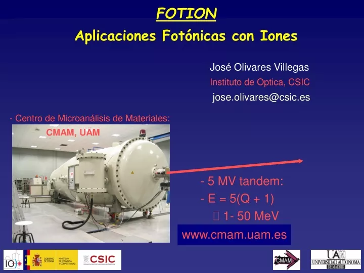
FOTION Aplicaciones Fotónicas con Iones. José Olivares Villegas Instituto de Optica , CSIC jose.olivares@csic.es. Centro de Microanálisis de Materiales: CMAM, UAM. 5 MV tandem: E = 5(Q + 1) 1- 50 MeV. www.cmam.uam.es. F 22 MeV. 3 μ m.

E N D
FOTION Aplicaciones Fotónicas con Iones José Olivares Villegas Instituto de Optica, CSIC jose.olivares@csic.es • Centro de Microanálisis de Materiales: CMAM, UAM • 5 MV tandem: • E = 5(Q + 1) 1- 50 MeV www.cmam.uam.es
F 22 MeV 3 μm • Modification of the optical properties of materials with ions • Swift heavy ionsforPhotonicsapplications • Electronicdamagefornano- and micro-structuring • Nanostructures ( optics…) • Optical waveguides ions LiNbO3 Olivares et al. APL, 2005 Crespillo et al. NIMB 267, 2009
Thermal Infrared camera: • In-situ surface temperature CCD colour camera: • For alignements and • Beam homogeneity with ionoluminescence Window at 45º to ion beam
Accurate control beam homogeneity (CCD-camera) Precise control sample temperature (IR camera) Ion-luminescence
Ion-matter interaction. Energy loss or stopping power, Se,n (keV/nm) LiNbO3 CMAM range Highenergy heavy ions (E 0.1MeV/amu) HighelectronicExcitation Highenergydensity Damagetracks It is valid for thin films or at the surface • Nuclear • damage • Electronic excitation
At CMAM (SRIM-2006) From ion implantation to ion irradiation • 5 MV tandem: E = 5(Q + 1) 1- 60 MeV • H, He… F, Si, …Cu, …Au Ion irradiation Se > Threshold Amorphous nano-tracks
Substrate Ion implantation Waveguides by optical barrier Standard model H, He MeV Optical barrier n: 1-10 % Guided mode Refactive Index 0 2 4 6 Depth (microns)
At CMAM (SRIM-2006) Novel Optical Waveguides by Ion Track Technology High-energy heavy ions or swift heavy ions
Ultrafast spike: thermal and excitation… T Tm • Se > Sth : Amorfización • Se < Sth : Defectos r (nm) I O N Se Sth Core Halo Ra z (μm)
TEM: Microscopía electrónica de transmisión TEMimages of Cu 51 MeV irradiated LiNbO3 . (a)The light stripes indicate the unetched tracks induced by ion bombardment;insets show the diffraction patterns; (b) HRTEM image showing etched nanopore in cross sectional view.
Tracks of huge aspect ratio 100x100 nm (2X2 mm) 5 nm / L1000 nm (= 0,1 / 20 mm)
Novel Optical Waveguides by Ion Irradiation Se Sn cm-2 2e14 4 μm Air Crystal 1e15 F 22 MeV LiNbO3 Sub-threshold Optical microscopy polished edge Fluences ~ 1014 at/cm2 lower a factor >102 !! Appl. Phys. Lett, 2005
RBS-channeling (H 3 MeV) Desorden estructural
1x1014 cm-2 3x1015 cm-2 Z X Y IONS LENS Micro-Raman spectroscopy (F. Agulló-Rueda, ICMM-CSIC) laser J. Olivares et al. J. Appl. Phys. (2007)
Novel Optical Waveguides by Ion Irradiation • 1 0.1 dB/cm • Perfiles de indice “step-like” Dispositivos no lineales con fluencias bajas, 1014 vs 1017at/cm2!!
Random isolated impacts at the surface y Guided mode z x Cl 46 MeV Optical waveguides Swift heavy ion irradiation Single track regime Threshold ?: A. Meftah et al, NIMB 237 (2005) Nanoestructured medium
Optical Waveguides Swift Heavy Ion Irradiation Cl 46 MeV ( = 633 nm) • Fluencias ultrabajas: 1012 at/cm2 !! Producción masiva
Nano-hills Expansion of amorphous nanotrack (810 x 550) nm Nano-track Ion Irradiation: Nanohills Nanopores Cu 50 MeV LiNbO3 y, z x AFM image
TEM: Microscopía electrónica de transmisión TEMimages of Cu 51 MeV irradiated LiNbO3 . (a)The light stripes indicate the unetched tracks induced by ion bombardment;insets show the diffraction patterns; (b) HRTEM image showing etched nanopore in cross sectional view.
Topography Irradiation: Br 46 MeV, 1e8 cm-2,Etching: HF 40% , Liquid, 30 min, at 55 °C Irradiation: Br 46 MeV, 1e8 cm-2,Etching: HF 40% , Vapor, 1 min, at 25 °C Silica LiNbO3
FOTION Aplicaciones Fotónicas con Iones jose.olivares@csic.es • Centro de Microanálisis de Materiales: CMAM, UAM • 5 MV tandem: • E = 5(Q + 1) 1- 50 MeV www.cmam.uam.es
FOTION Aplicaciones Fotónicas con Iones… + láser! jose.olivares@csic.es www.cmam.uam.es Láser pulsado: ~ 100 fs 6 mJ/pulso x 1 kHz = 800, 400 y 266 nm