Download
1 / 22
330 likes | 696 Views
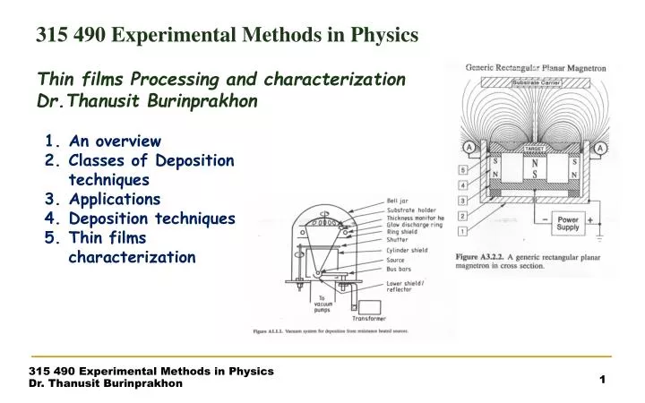
315 490 Experimental Methods in Physics Thin films Processing and characterization Dr.Thanusit Burinprakhon. An overview Classes of Deposition techniques Applications Deposition techniques Thin films characterization. What is thin film?.

E N D
315 490 Experimental Methods in Physics Thin films Processing and characterization Dr.ThanusitBurinprakhon An overview Classes of Deposition techniques Applications Deposition techniques Thin films characterization
What is thin film? • Thin film is referred to a thin layer of a material deposited on a surface of a host material (substrate). • Thickness < 100 mm • 500 nm of gold layer deposited on a glass slide: gold = thin film, glass slide = substrate • What is thin film processing and technology? • A process and technology to produce a materials in form of thin films on a given substrate. • Aims to fabricate thin films of materials for: • Properties investigation • Fabrication of thin film devices • Surface engineering: to control surface properties, increase performance, reduce costs, etc…, of a work piece Thin films processing and characterization 1. An overview
The market • Initiated in late 1950s, decoration coatings or surface-engineered products for toys, textiles, etc. • In 1989 • Equipment with an estimated value of $6 billion was produced worldwide in 1989 for thin film surface technology. • Components and devices manufactured with such equipment amounted to $60 billion • The value of the end-products which contained components made possible by surface engineering is estimated at $600 billion. • In 2011, these market figures continue to grow. Thin films processing and characterization 1. An overview
Why strong market? • R & D investment • Japan : spending $100 to $150 million for R/D in diamond and diamond-like carbon coatings. The payoff is estimated at $16 billion by the end of this decade. • US: more than $10 million have been spent in the for R&D in advance thermal barrier coatings by PVD methods for high temperature operation of turbine blades. • Wear-resistant coatings for disc and heads has attracted much more than $10 million in R/D expenditures worldwide. • Surface engineering remains a growth industry because it offers the potential to: • Creation of entirely new products. • Solve previously unsolved engineering problems. • Improved functionality of existing products. • Conservation of scarce materials. • Green technology • Nanotech Ready !!! Thin films processing and characterization 1. An overview
Physicists’ point of view Thin films processing and characterization 2. Classes of thin film deposition techniques
Chemists’ point of view Thin films processing and characterization 2. Classes of thin film deposition techniques
Optically Functional • Electrically Functional • Mechanically Functional • Chemically Functional • Decorative • Keys Applications (listed in 1982) • Optically Functional • Laser optics (reflective and transmitting) • architectural glazing • home mirrors • automotive rearview mirrors • reflective and anti-reflective coatings • optically absorbing coatings • selective solar absorbers • Optical discs Thin films processing and characterization 3. Applications
Electrically Functional • Electrical conductors • electrical contacts • active solid state devices • electrical insulators • solar cells • Mechanically Functional • Lubrication films • wear and erosion resistant coatings • diffusion barriers • hard coatings for cutting tools Thin films processing and characterization 3. Applications
Chemically Functional • Corrosion resistant coatings • catalytic coatings • engine blades and vanes • battery strips • marine use equipment • Decorations • Watch bezels, bands • eyeglass frames • costume jewelry Thin films processing and characterization 3. Applications
Frontier Applications • Reflective surfaces, e.g., for laser mirrors • Thermal barrier coatings for blades and vanes operating at high temperatures.\ • Thin film photovoltaic devices. • Hard protective coatings: diamond-like carbon for heads and discs • Sub-micron microelectronic devices. • Biomedical devices, e.g., neurological electrodes, heart valves, artificial organs • Ultrafine powders (go Nanotech !!!) • Data storage device (hard discs) • …… • and Many more ….. Thin films processing and characterization 3. Applications
Vacuum Evaporation • Evaporation chamber Thin films processing and characterization 4. Deposition techniques
Vacuum Evaporation • Heating elements Thin films processing and characterization 4. Deposition techniques
DC Glow Discharge Sputtering Thin films processing and characterization 4. Deposition techniques
Electron beam evaporator Thin films processing and characterization 4. Deposition techniques
Laser Ablation Thin films processing and characterization 4. Deposition techniques
Molecular Beam Epitaxy (MBE) Thin films processing and characterization 4. Deposition techniques
Magnetron Sputtering: Rectangular planar magnetron gun Thin films processing and characterization 4. Deposition techniques
Magnetron Sputtering: Circular planar magnetron gun Thin films processing and characterization 4. Deposition techniques
Aims: • Determining functionality and Establishing performance limits for a specific application • Establishing product acceptance specifications • Establishing a baseline for satisfactory composition, structure, or performance • Monitoring reproducibility of processing • Determining the stability of the material under service and degradation conditions • Assisting in failure analysis • Avoiding surprises Thin films processing and characterization 5. Thin film characterization
Characterization techniques: Thin films processing and characterization 5. Thin film characterization
Characterization techniques: Thin films processing and characterization 5. Thin film characterization
Characterization techniques: Thin films processing and characterization 5. Thin film characterization