Download
1 / 18
190 likes | 460 Views
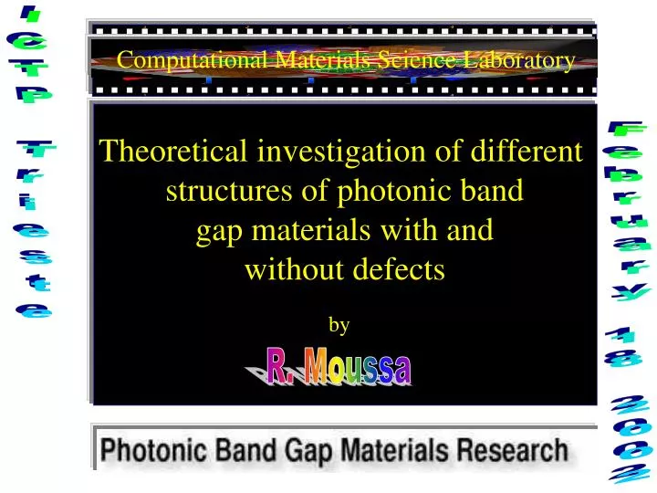
Computational Materials Science Laboratory. Theoretical investigation of different structures of photonic band gap materials with and without defects. ICTP Trieste. February 18 2002. by. R. Moussa. Theory. Results. Contents. The 2D hexagonal structures.

E N D
Computational Materials Science Laboratory • Theoretical investigation of different • structures of photonic band • gap materials with and • without defects ICTP Trieste February 18 2002 by R. Moussa
Theory Results Contents The 2D hexagonal structures What is a photonic band gap? The cavity concept and defect in 2D structures The numerical methods The 3D structures The 1D structures The Sc, cfc and inverted opal structures The semiconductors multilayers The 2D structures
Computational Materials Science Laboratory What is a photonic crystal? ICTP Trieste A simple definition February 18 2002 A physical definition a Photonic Band Gap Material
Computational Materials Science Laboratory What is the physical origin of the photonic band structure? ICTP Trieste Electronic The electron wave scatters coherently from the different potential regions The electromagnetic fields scatter coherently at the interfaces between different dielectric regions February 18 2002 Photonic
Computational Materials Science Laboratory a a a a b b b b What are the conditions to have a PBG? ICTP Trieste 1 The crystal periodicity February 18 2002 A system of stacking layers of high and low refractive index
Computational Materials Science Laboratory 2 A minimum of the contrast index ICTP Trieste February 18 2002
Computational Materials Science Laboratory a a a a b b b b Theoptical wave is of the same magnitude as the stack periodicity 3 ICTP Trieste a February 18 2002
Computational Materials Science Laboratory 4 Thesymmetry of the lattice structures ICTP Trieste 2D 3D 1D February 18 2002 The face centered cubic crystal (3D) was considered the best candidate since this structure has the most spherical Brillouin zone.
Computational Materials Science Laboratory Why it is so important? ICTP Trieste The spontaneous emission control February 18 2002
Computational Materials Science Laboratory antenna ( a ) trapped radiation air substrate air (b) antenna air photonic crystal substrate air Why it is so important? ICTP Trieste High reflection substrate based on PBGM A simple substrate February 18 2002 A substrate based on photonic crystal
Computational Materials Science Laboratory Why it is so important? ICTP Trieste Highly efficient light emitting diodes Spontaneous emission LED p-n junction Redirect the photons February 18 2002 2% of light 90-100% each e- on 1 photon
Computational Materials Science Laboratory Why it is so important? ICTP Trieste Increase the spontaneous emission Edward Purcell 1946 February 18 2002 Increase the emission cavity Inhibition of the propagation PBGM
Computational Materials Science Laboratory When we introduce the defect ICTP Trieste Introducing a cylinder with different radius Introducing a cylinder with different dielectric constant February 18 2002 by either adding or removing dielectric material from a chosen unit cell in the crystal.
Computational Materials Science Laboratory Consequences ICTP Trieste Have cavities with high quality factors Show quite narrow transmission spectra leading to high filters February 18 2002 resonant cavities is enhancing the efficiency of lasers
Computational Materials Science Laboratory Waveguide application ICTP Trieste micro-waves Metallic waveguide coaxial cables visible February 18 2002 Optical fibers Principal: Rely on total internal reflection.
Computational Materials Science Laboratory problem ICTP Trieste If a fiber optic cable takes a tight curve, the angle of incidence is too large for total internal reflection February 18 2002 photonic cristal Since they do not relay exclusively on total internal reflection, continue to confine light even around light corners.
Computational Materials Science Laboratory Light that propagates with frequency within the PBG of the crystal is confined, and can be directed along the waveguide. ICTP Trieste February 18 2002 Light is forced to bounce around inside the waveguide, so the light is guided only around corners.
Theory Results Contents The 2D hexagonal structures What is a photonic band gap? The cavity concept and defect in 2D structures The numerical methods The 3D structures The 1D structures The Sc, cfc and inverted opal structures The semiconductors multilayers The 2D structures