Download
1 / 36
370 likes | 529 Views
Stanford Synchrotron Radiation Laboratory. More Thin Film X-ray Scattering: Polycrystalline Films. Mike Toney, SSRL. Introduction (real space – reciprocal space) Some general aspects of thin film scattering Polycrystalline film (no texture) – RuPt Some texture film - MnPt Summary

E N D
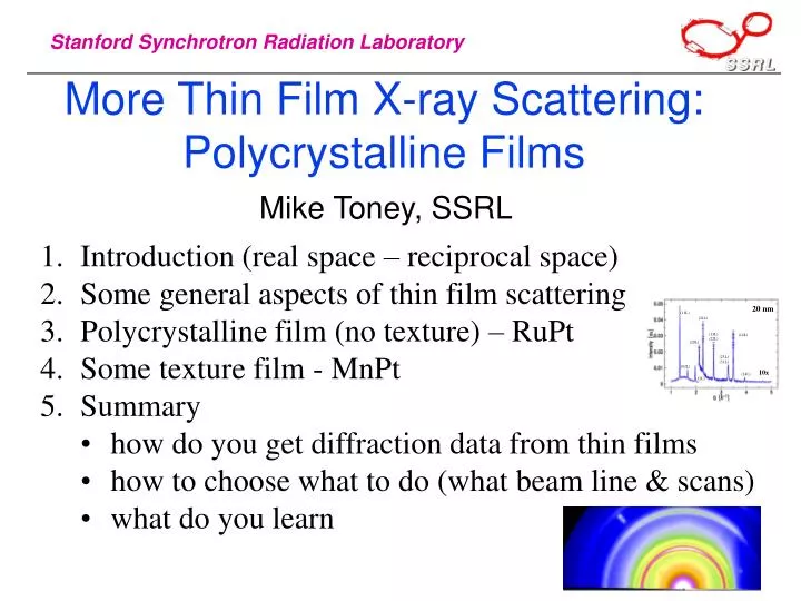
Stanford Synchrotron Radiation Laboratory More Thin Film X-ray Scattering: Polycrystalline Films Mike Toney, SSRL • Introduction (real space – reciprocal space) • Some general aspects of thin film scattering • Polycrystalline film (no texture) – RuPt • Some texture film - MnPt • Summary • how do you get diffraction data from thin films • how to choose what to do (what beam line & scans) • what do you learn
Real and Reciprocal Space Reciprocal space Real space epitaxial film Arturas spots “powder” film (polycrystalline) spheres
(0 2) (-1 1) (1 1) (0 1) (2 0) (-2 0) (-1 0) (1 0) (0 -1) (1-1) (-1 -1) (0 -2) Diffraction Pattern: Powders Q “Powder”: random orientation of many small crystals (crystallites) (20) (10) (02) Intensity Q
Real and Reciprocal Space textured film Reciprocal space Real space side rings top slice gives spots differences in extent of texture
(0 2) (-1 1) (1 1) (0 1) (2 0) (-2 0) (0 2) (-1 2) (1 2) Qxy (-1 0) (1 0) (0 -1) (1-1) (1 1) (-1 -1) (-1 1) (2 0) (-2 0) (0 -2) (1-1) (-1 -1) (0 -2) (1 -2) (-1 -2) Textured Thin Film textured 2D Powder: oriented normal to surface random orientation of crystals in substrate plane rings
Thin Film Scattering: what do I do? • what beam line? (2-1, 7-2, 11-3) • area vs point detector, nature of sample • energy & flux • what scans? (“where” in reciprocal space) • what do you want to learn? • what kind of sample (epitaxial, textured)? • phase identification • lattice parameters • defects • texture • crystallite size • atomic structure
2q Q Thin Film Scattering Two ways: Area detector & Point detector
Cu Intensity Q Polycrystalline (powder) film “Powder”: random orientation of many small crystals (crystallites) Q What scans: • what Q range to scan? • what direction for Q? • rocking mode? • avoid substrate peaks • best signal to noise • fast or accurate?
(111) (200) (111) (110) (220) Textured Thin Films Texture: preferred orientation of crystallites rings What scans: • what Q range to scan? • what direction for Q? • texture determination? Q • avoid substrate peaks • Q goes through peaks • best signal to noise • fast or accurate? slice gives spots
RuPt Thin Films Direct Methanol Fuel Cell (DMFC) • low operating temperature & high energy density • low power applications (cell phones, PCs,) RuPt alloys used as catalysts for DMFCs • as nanoparticles, but also films • catalytic activity of RuPt depends on composition and structure (hcp or fcc) anode: CH3OH + H2O => CO2 + 6H+ + 6e- cathode: 3/2O2 + 6H+ +6e- => 3H2O sum: CH3OH + 3/2O2 => CO2 + 2H2O Hamnet, Catalysis Today 38, 445 (1997) Park et al., J. Phys. Chem. B 106, 1735 (2002)
RuPt: vary % Si RuPt Thin Films Goal: Correlate crystal structure of RuPt alloys to catalytic activity Pt is fcc; Ru is hcp fcc->hcp transition as Ru increases thin films of RuPt rf sputtered 13 nm thick • T-W Kim, S-J Park, Gwangju Institute of Science & Technology, South Korea • K-W Park, Y-E Sung, Seoul National University, South Korea • Lindsay Jones, (SULI Internship)
Intensity Q Polycrystalline (powder) film “Powder”: random orientation of many small crystals (crystallites) Q what do you want to learn? • phase identification • lattice parameters • defects • crystallite size choose scans to: • avoid substrate peaks • best signal to noise
RuPt Thin Films Area detector Area Detector 2q incident scattered Q ~ 0.4-0.5 deg Grazing incidence: • limits penetration in substrate (avoids substrate peaks) • fast Si RuPt
Detector Q Area Detector incident scattered 2q incident scattered Q small RuPt Thin Films Area detector on beam line 11-3
RuPt Thin Films Ru(72) Pt (28) fcc(311) & (222) glitch Q fcc (220) fcc (200) Q fcc (111) in-plane scan use fit2d (or other) to integrate
Si RuPt GIXS Thin Films Q = k’ – k ;parallel to surface Grazing incidence: • planes parallel to surface • limits penetration in substrate
RuPt Thin Films: diffraction • accurate, but slow • increasing Ru => transition from fcc to mixed fcc/hcp to hcp T-W. Kim et al., J. Phys. Chem. B 109, 12845 (2005)
RuPt Thin Films: diffraction Fit peaks to get: • peak positions => lattice parameters • peak widths => grain (particle) size • integrated intensities => phase fraction (hcp vs fcc)
RuPt Thin Films Use peak intensities to quantify phases Thin Film Phase Diagram Thin film different from bulk, due to sputter deposition Kinetics do not allow equilibrium
RuPt Films: Lattice Parameters • Accurately determine lattice parameters • Cannot use bulk alloy lattice parameters to get composition bulk alloys
Summary: polycrystalline RuPt films: phase identification (hcp, fcc) correlate structure to activity (hcp RuPt does not adversely affect activity) lattice parameters (strain) no strong texture crystallite size
$0.0003/MB $5.2/MB Thin Films for Magnetic Recording Write Head Read Head 2 mm Tsann Lin and Daniele Mauri, Hitachi Global Storage Mahesh Samant, IBM 500 nm Pinned Ferromagntic Film
Thin Films for Magnetic Recording Exchange bias (Heb) current flow • Understand this behavior (for MnPt) Toney, Samant, Lin, Mauri, Appl. Phys. Lett. 81, 4565 (2002)
Mn Mn Pt MnPt Films: chemical order chemically disordered fcc structure not antiferromagnetic chemically ordered L10 structure (face centered tetragonal) c/a = 0.92 antiferromagnetic (TN = 700-800o C) Cebollada, Farrow & Toney, in Magnetic Nanostructures, Nalaw, ed. 2002
Mn a MnPt Films: chemical order chemical order parameter (S): extent of chemical order partial chemical order: S=1/2 Full chemical order: S=1 No chemical order: S=0 S=0 S=½ S=1 (111) (111) (200) (200) (200) (111) (202) (202) (220) (220) (110) (220) (110) (001) (002) (002) (001) determine S from peak intensities (110)/(220) ratio Cebollada, Farrow & Toney, in Magnetic Nanostructures, Nalaw, ed. 2002
(111) (200) (111) (110) (220) Textured Thin Films sputter deposition annealed at 280C for 2 hours What scans? What do you want to learn? • phase identification • crystallite size • texture Q What to: • avoid substrate peaks • best signal to noise
(111) (220) (110) Q MnPt Films: diffraction Si MnPt Q = k’ – k ;parallel to surface 2θ is scattering angle α = incidence angle β = exit angle Grazing incidence: • planes parallel to surface • limits penetration in substrate
(111) (220) (110) Q MnPt Films: diffraction • increased thickness: the superlattice (001) and (110) peaks increase => more chemical ordering • coexistence of fcc and L10 Toney, Samant, Lin, Mauri, Appl. Phys. Lett. 81, 4565 (2002)
Mn MnPt Films: chemical order S = extent of chemical order S=1/2 S=1 S=0 Calculate S from (110)/(220) intensity ratio: S = A[I(110)/(fPt-fMn)2]/[I(220)/(fPt+fMn)2] I = integrated intensity of peaks A = Q dependent term f = atomic form factor Calculate fcc & L10 fraction form fcc(220) and L10 (220)/(202): fcc fraction = B*I(fcc)/[I(fcc) + I(L10)] B is Q dependent term close to 1.0 Cebollada, Farrow & Toney, in Magnetic Nanostructures, Nalaw, ed. 2002
MnPt Film Structure • coexistence of fcc and L10 MnPt(inhomogeneous) • complete chemical order for highest Heb
Q (111) (220) (110) MnPt Films: crystallite size diameter = 2π*0.86/fwhm(Q) more chemically ordered MnPt -> larger grains NiFe & Cu do not change much with annealing
Texture in Thin Films • Pole figure measures orientation distribution of diffracting planes • Ψ = 0 deg planes along substrate • Ψ = 90 deg planes ┴ to substrate
(111) Q (111) (110) MnPt Films: Texture annealing effect thickness effect width ca 5-10 degs
(111) (200) (111) (110) (220) MnPt Thin Films: Summary MnPt films: phase identification (L10, fcc) crystallite size texture determination • Scan choice requires knowledge of reciprocal space & what you want to learn • thin MnPt remains fcc => not antiferromagnetic and no exchange bias • coexistence between fcc and L10 (inhomogeneous) • need complete L10 order to get highest exchange • grain growth and change in preferred orientation with development of chemical order => L10 forms by nucleation & growth
Summary • what do you want to learn? • phase identification • lattice parameters • defects • texture • crystallite size • atomic structure • what kind of sample (epitaxial, textured)? • what beam line? (2-1, 7-2, 11-3) • what scans? (“where” in reciprocal space)