Download
1 / 33
330 likes | 549 Views
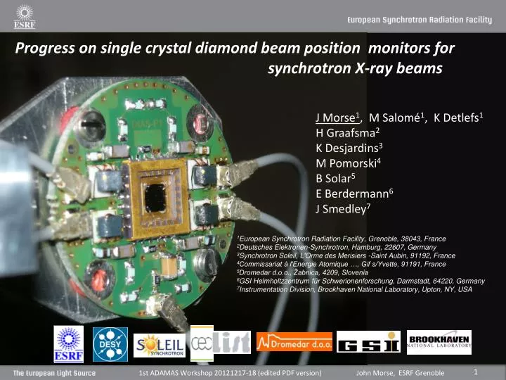
Progress on single crystal diamond beam position monitors for synchrotron X-ray beams. J Morse 1 , M Salomé 1 , K Detlefs 1 H Graafsma 2 K Desjardins 3 M Pomorski 4 B Solar 5 E Berdermann 6 J Smedley 7. 1 European Synchrotron Radiation Facility, Grenoble, 38043, France

E N D
Progress on single crystal diamond beam position monitors for synchrotron X-ray beams J Morse1, M Salomé1, K Detlefs1 H Graafsma2 K Desjardins3 M Pomorski4 B Solar5 E Berdermann6 J Smedley7 1European Synchrotron Radiation Facility, Grenoble, 38043, France 2Deutsches Elektronen-Synchrotron, Hamburg, 22607, Germany 3Synchrotron Soleil, L'Orme des Merisiers -Saint Aubin, 91192, France 4Commissariat à l'Energie Atomique …, Gif s/Yvette, 91191, France 5Dromedar d.o.o., Žabnica, 4209, Slovenia 6GSI Helmholtzzentrum für Schwerionenforschung, Darmstadt, 64220, Germany 7Instrumentation Division, Brookhaven National Laboratory, Upton, NY, USA
Outline • 1. Synchrotrons and X-ray beam monitoring needs: • why diamond? why single crystal? • CVD single crystal diamond bulk- and surface- challenges • ---------------------------------- • quadrant- and resistive-electrode devices: • principle of operation; fabrication; • ‘near dc ’ (electrometer) and RF readout methods • 5. 'superthinning’ project • 6. Conclusions / status
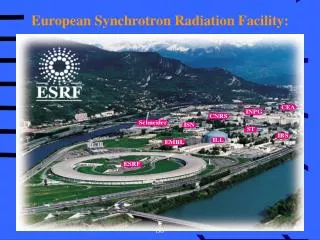
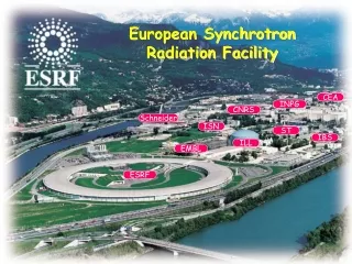
ESRF-Grenoble, France synchrotron sources: Now (2012) about 50 major X-ray synchrotrons in the world… sources of infra-red to MeV photon beams, but main interest 1 ~ 100keV the big three, commissioned early 1990's… APS-Argonne nr. Chicago SPring8, Harima nr. Osaka 3
synchrotron sources: situation in 2012 J-L Revol, ESRF (ASD)
energy tunability ESRF Ø300m undulator source ΔE/E ~10-2 50~100m source to end station white/pink beam 0.1~1kWmm-2 monochromatic beam ~mW beam position - intensity monitors 3rd generation synchrotron beamlines ~ 45 beamline stations ‘white’ X-ray beam Bragg diffraction from silicon crystals monochromatic X-ray beam out pink/white beam ΔE/E~10 -4 flux on sample ~1013 ph/sec
Position required beam stability ~10% of 0.1 ~ 50μm beam size NINA upgrade beamline, nanofocusing → 10nm beam on sample measurements ~dc (thermal drifts) to ~ 1kHz (acoustic vibrations) Intensity: accuracy & linearity requirement typically ≤ 1% (sometimes <0.01% ratiometric) (sub) millisec sampling; pump probe synchronization <100psec Timing: device… continuous signal readout with negligible beam interference: absorption, coherence loss, scattering beamline compatibility: package size, operation in air, dirty-vacuum, clean-UHV lifetime >months under ionizing radiation loads to >104 Gray/sec X-ray beamline monitoring goals crystal monochromatized beams : device absorbed X-ray power ≤ few mW but beam powers to 100Wmm-2 (C-W) in undulator ‘white’ beams: heat load → ONLY possible with diamond
why diamond ? Z = 6 → low X-ray absorption by photoelectric effect … ~8-fold less than silicon for 10keV X-rays …at energies >20keV, short range of Compton-electrons • 5.5eV bandgap • →‘zero’ leakage current at room temperature and at high E-fields • → nanosec pulse response times • →insensitive to ambient light, (λc ~ 215nm ) - ‘all diamond’ devices are (X-ray) radiation hard --no atomic displacement damage • extreme thermal conductivity: • diamond ~2000 Wm-1 °K-1 at 273°K , cf. silicon ~150
quadrant diamond X-ray beam monitor: principle photocurrent readout of beam position and intensity →simple, compact devices beam • high purity diamond plate ~10…100µm thick • metal surface electrical contacts ~100nm thick ( e.g. Al, Pt, W) • externally applied bias field 0.5 ~5 Vµm-1 • directly intercepting beam, diamond bulk acts as solid state ‘ionization chamber’ • electron thermalization range a few µm for <20keV X-rays DIAMOND • photocharge drifts for ~ nanosecond in applied E field to electrodes • charge cloud lateral thermal diffusion ~10µm surface contact →induced signals can be measured with 'integrating' electrometer (charge), or drift current pulses observed directly (wideband) …beam 'center of gravity' determined by interpolation
why not polycrystalline diamond? Polycrystalline: attractive: 6" wafers available → easier, cheaper device processing XBIC: signal current map made from x, y raster scan of sample with a ~7keV micron-focused X-ray beam but crystallite grain-boundaries of size ~ 10% of film growth thickness → random crystallite orientations 'powder ring' X-ray scattering… → local field distortions and charge trapping & signal response lag LIST-CEA Saclay data (ESRF ID21)
Charge collection efficiency ~1…10%, variable (prompt + detrapped components) with applied E field 1…5 V/µm, polycrystalline diamond: trapping andsignal lag signal decay after beam cut off 10 sec SLS MX beam 15 x 100µm2, 1.3 x 10¹² ph/sec at 12keV data Ralf Menk, 2006: polycrystalline ~10µm thick, grown on Si substrate by Diamond Materials GmbH, Freiburg, contacts fabricated at PSI Nanofab (?)
Platinum electrodes M edge feature: photons absorbed by incident contact (no field dependence observed) Carbon K edge feature is field dependent, caused by incomplete carrier collection for near surface absorption electrical responsivity with X-ray energy responsivity J. Keister and J. Smedley, NIM A 606, (2009), 7
1.E+00 1.E - 01 1.E - 02 1.E - 03 1.E - 04 1.E - 05 Gas ion chamber calibration 1.E - 06 Calorimetric calibration 1.E - 07 Fit, w = 13.4 +/ - 0.2 eV 1.E - 08 1.E - 07 1.E - 05 1.E - 03 1.E - 01 1.E+01 power Absorbed by Diamond (W) signal linearity with beam flux Linearity at high currents, single crystal diamond with Pt electrodes (measurements at BNL NSLS-X28C white beam, absorbed power density up to 20 Wmm-2) ESRF ID21 microbeam, 7keV 20nm+20nm - GSI Cr-Au contacts 10pA diamond signal (Amps) J. Bohon, E. Muller, J. Smedley, J. Synch. Rad 17, (2010) at ESRF, signal linearity observed over range ~10pA to >10µA (monochromatic beams, 7 - 20 keV data) → operation in linear mode shown over total >10 orders magnitude
Y X A B C D Packaged device, ESRF ID09B, ID11, Desy tests position measurement: multiple electrodes: exploits diffusion splitting (~10µm) of charge between A, B, C, D contacts of quadrant motif → difference/sum of currents A, B, C, D gives beam 'centre of gravity’ * → sum of currents gives beam intensity *requires high signal/noise !
position measurement: resistive contacts signal current is shared between edge strip electrodes as ratio of resistances through resistive contact → linear position response possible over several millimeters → true beam center of gravity, so position sensitivity independent of beam size variation signal/noise may be limited by contact resistance, slower response (RC ~µsec) first device used in ESRF & Soleil beam tests ~2009
Inex - ESRF - DESY RF readout design ~100nm Al contacts on 30 and 100µm diamonds OSU-Kagan quadrant designs: contact fabrication DIC microscopy Lift-off lithography: cf. shadow mask deposition: -allows complex geometric designs for metal contacts; -multiple designs on single mask; -electrode features to < 1µm …but difficult work on small samples -surface preparation, hot acid cleaning and post-clean handling - edge ‘beading’ of spin deposited resist ~100nm Al contacts on 100µm plates INEX, UK ESRF-DESY-OSU XBPM and microdosimetry mask set , 2010 white light microscopy
ESRF ID21 beam ~0.6x1.5µm2, ~4x10⁹ph/sec at 7.2keV, cross polarizer-selected e6 plates, two-side ion beam etched to final 100µm thickness, 100nm Al sputtered contacts using lift off lithogaphy (OSU-Kagan, 2010) full charge collection for >10V bias (0.1Vµm-1) dark leakage current <0.1pA (measurement sensitivity limit) at 200V bias no hotspot defects found over 7mm2 contact areas for 3/3 preselected samples tested single crystal I-V response in X-ray beam calibration relative to silicon diode →εDiamond = 13.05 +/-0.2 eV/e-h pair
Line scan @ 7.2keV beam collimated 200µm 1 2 signal slope ~0.5% /micron For a small beam (< 5µm), crossover response is ~independent of beam size: convolution of photoelectron thermalization range and lateral charge diffusion occurring during carrier drift …beam focused <1µm isolation gap ~120µm signal slope ~5% /micron position response of diamond quadrant devices For large beamsize (> 50µm), device ‘crossover response’ is simply the line integral across the beam intensity profile 2 1 ESRF ID21 electrometer ‘charge integral’ measurements, i.e. signal integration time >> charge carrier drift time
4.4 hours synchrotron orbit shifts, or something upstream on beamline… beamline tests : position timescan and ‘vibrations’, ESRF ID09B, single bunch mode (355kHz) charge generated in diamond ~ 0.1pC/pulse currents measured by Keithley 485 electrometers (10Hz BW, mean current measured ~10µA/contact) 390um thick diamond sample ‘S361-1’ with TiW quadrant contacts inserted before final slitbox, pink undulator beam peaking at 20keV
… Al electrode contacts and wire bonding (Kagan – OSU 2010) homogeneous response map for 3/3 samples tested, no signal ‘hot spot’ defects <0.1pA leakage current at 2Vµm-1 vertical streaks are from beam Io normalization errors during scan compact diamond mounting ESRF-ID21 Fluorescence Microscopy beamline: limited space, operation in dirty vacuum and in air IBM-etched e6 single crystals 4.2 x 4.2mm2, thicknesses 30 & 100µm Rogers multilayer PCB, microcoax wire leadouts 10mm o scan stage guard-ringed direct PCB mounting with … f ocused beam sample x,y piezo stage ID21 beam line installation diamond r a M quad n t B P
vertical ) µm horizontal 1.0 position* ( 0.5 0.0 -0.5 -1.0 -1.5 0 5000 10000 15000 20000 25000 30000 35000 *scaling 'calibration' error possibly ~10% time (sec) quadrant device, electrometer readout: time scans ESRF ID21 FZP microfocus beam tracking 1sec/point: vertical beam jumps on synchrotron e-beam refills ~40% synchrotron refill σ =13.3nm 1sec V-F 2010 data, 4x10⁹ph/sec at 7.2keV (FZP → K-B mirror) 14(18)nm vertical(horizontal), 1sec integration 33(48)nm, 0,1 sec integration σ= 20.4nm 1sec V-F X-ray flux ~108 ph/sec at 7keV (FZP optic): ~ 20fC in diamond per X ray bunch ~ 10nA ‘dc equivalent’ signal current
ID22 nanofocus beamline: stability measurements 5-6 Sept 2012: x 17keV, flux 2.5x 10⁹ ph/sec 17keV, flux 2.5x 10⁹ ph/sec 25µm 17keV beam nnx 1010 ph/sec x x 23:00, successive time scans: blue data: beam focused (~50nm) on diamond 'sample' red data: diamond axially displaced 5mm
ID22 nanofocus beamline: stability measurements 17keV, flux 2.5x 10⁹ ph/sec short term vertical and horizontal stabilities 17keV, flux 5.0 x 10⁹ ph/sec (16 bunch mode) Keithley 485 electrometers, 100msec integrations at ~1.6sec intervals diamond piezo stage step-displaced vertically: 10nm steps clearly visible 2.5nm rms quasi-linear crossover response over ~8µm beam absorption in diamond 1.8% (~70% via photoelectric effect) measured quadrant currents sum <i > 13nA (ESRF 16 bunch mode, peak pulse currents ~2µA) for photoelectric absorption, i = ɸ x Exray / ε (Amps) ɸ = absorbed X-ray flux; EX-ray = photon energy (eV) ε = diamond e-h pair production energy = 13 eV 3.9nm rms
‘resistive contact’ BPMs 40µm e6 plate, with sputtered diamond-like carbon (DLC) contacts (CEA-LIST, M. Pomorski), ESRF-ID06 beam test: I-V response in 10.5keV beam, ~1011 ph/sec (~0.5µA measured photocurrents) complete charge collection for bias >5V non-injecting contact (measured to +/-100V) metal electrodesAl, TiPtAu DLC resistive layer intrinsic diamond slab DLC resistive layer DLC resistive layer metal collecting electrodes resistivity of contacts ~`20kΩ/square, physically hard and scratch resistant layers 0.2µm thickness long term radiation, temperature stability…?
resistive contact BPM: device #2 at ESRF-ID06 Position noise of first device tested at ESRF measured was limited by the 20kΩ resistance of the DLC contacts (electrometer input voltage noise driven currents) new device installed at ID06 June 2012, 265µm thick, 170-200kΩ resistance contacts shadow-mask Au electrodes over full-surface DLC PCB mounted over hole and electrodes connected by Ag loaded thermoplastic signal current reaches a well defined plateau corresponding to complete photo-charge collection. excess signal current and noise seen with >100V 'negative' bias -->local diamond bulk defect(s) device works perfectly with positive bias…
performance, device #2 at ESRF-ID06 beam 12keV, 1.3x 10¹³ph/sec, ~25x25µm2 device linearity across entire 2mm spacing between the gold line contacts ~zero horizontal-vertical crosstalk (orientation alignment errors?) x,y mesh plot shows uniform response over most of the 2x2 mm2 active area: no local defects. differences between red and blue data points are from beam vertical position drift occurring during two x,y mesh scans of the BPM.
duo-lateral Resistive Electrode, position resolutions device #1, 20 kΩcontacts, 40µm thick diamond, S/N ~104 (electrometer offset induced noise limit) active area 2 x 2 mm2, 100msec integrations σ = 258nm [µm] [µm] ID06 1 MΩcontacts,300µm thick diamond, S/N ~105, active area 2.5 x 2.5 mm2, 100msec integrations σ = 27nm Proxima2
narrowband RF readout: Libera Brilliance beam X, Y, Σ out over fast network 1 2 3 4 pulse signals in ~500 systems installed at ESRF + DESY for electron orbit stabilization using capacitive pick-up buttons analog stage: SAW narrowband tuned filter (352MHz ESRF, 500MHz DESY) digital sampling at 110MHz, FPGA digital filtering → output data stream ~130ksample/sec 'rotating' crossbar RF switch removes electronic drift between A,B,C,D input channels
signal vs. detector bias (390µm thick sample, 50µm isolation gap 550V 217V 138V narrowband RF readout, first tests Quadrant electrode device first test at DESY-DORIS F1 (white bending magnet, Al filtered beam May 2012 monochromatic beam tests at DESY P11 with 100µm thick plate electrode ground bounce crosstalk higher field, thinner plate → shorter transit times ( <2ns ) !! with Libera brilliance system, measure 'narrowband' (~5MHz BW ) power at 500MHz center frequency →only measure ‘ fast drift’ signal components
Libera dynamic position response µm µm first test at DESY Doris synchrotron white beam (filtered bending magnet F4) stability timescan (Libera ADC buffer data, 130KHz readout digital sampling-averages) rms position noise* vs. bandwidth ground shock in position noise includes real beam-sensor movements • J. Morse, B. Solar and H. Graafsma, J. Synchrotron Rad. 17, 456‐464 (2010)
RF readout tests DESY Petra P11 (May 2012) Tests of series of 8 quadrant BPMs (OSU- and INEX-fabricated Al electrodes) beam vibrations measured 30m from monochromator with bad LN cooling turbulence beam ~ 50x100µm2 ~1013 ph/sec, 10.0keV quadrant BPM on PCB with 500MHz LC resonators and transformer cable impedance matching Si diode Q1 diamond BPM-1 Q2 diamond BPM-2 Q3 Q4 20mV, 5ns /div DSO traces, 'wideband' after 500MHz LC filter (A+B-C-D)/(A+B+C+D) 130 ksamples/sec (digital averages) BPM 1 BPM2 x, y raster scan of electrode responses, Libera data (sum map) time (secs)
Superthinned diamond membrane beam monitors 40µm thick plate shows significant trapping – I-V plot with X-ray beam shows no plateau region … …but 7µm membrane area has a good I-V plateau , i.e. bulk trapping in membrane is at ‘acceptable’ level fast response and no polarization effects seen can we use material with ~ppm N impurity ?? DDK scaife-polished optical grade CVD single crystal (optical grade material!) selected for low wedge error cental area thickness ~3µm after ArO etching membrane survived boiling acid clean and Al electrodes deposition ceramic mounting/wire bonding (Systrel, Paris) tested at Soleil Synchrotron October 2012 see talk of Michal Pomorski, this workshop
conclusions / status / future: • for intensity and position measurements, ‘proof of principle’ now well established by several groups • using quadrant devices, with electrometer or RF signal readout approaches • quality of CVD single crystal material --threading dislocation clusters-- remains a serious limit on • device yield (bad samples shows high dark signal currents and local signal ‘gain’ effects…) • Element Six ‘electronic grade’ samples have not improved over past ~7 years • → selection of material still necessary to avoid local 'hotspots' • ongoing work: • - testing / deployment of devices: electrometer readout at ESRF; Soleil… RF readout at Petra; NSLS-BNL • - investigating commerical fabrication (INEX; Micron; …) for series production of 'standard' device(s) • and sourcing of superthin plates <10µm by deep dry etching • - robust contacts and devices: - DLC variants for resistive contacts - boron doped CVD overgrowth - passivation (Al3N4; SiOx …?)