Download
1 / 47
510 likes | 814 Views
Analog to Digital in a Few Simple Steps A Guide to Designing with SAR ADCs Miro Oljaca Senior Applications Engineer Texas Instruments Inc Tucson, Arizona USA moljaca@ti.com. SAR ADC’s Block Diagram. Sample & Hold Amplifier. Sampling Signal. Equivalent Input Circuit.

E N D
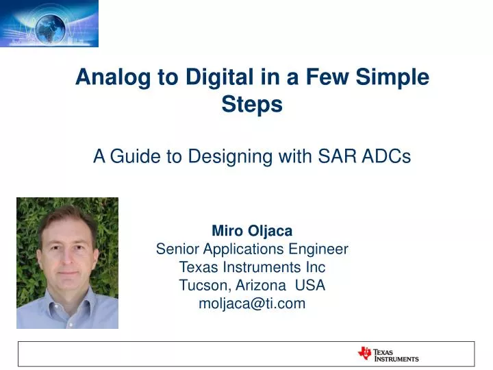
Analog to Digital in a Few Simple Steps A Guide to Designing with SAR ADCs Miro Oljaca Senior Applications Engineer Texas Instruments Inc Tucson, Arizona USA moljaca@ti.com
SAR ADC’s Block Diagram Sample & Hold Amplifier Sampling Signal
Equivalent Input Circuit From the Data Sheet for ADS8326: - Sampling capacitor is 48pF - Sampling switch resistance is 50Ω
Voltage Ripple on The Input of ADC Sampling Signal Analog Input Signal
Settling Time as a Function of Time Constant VCSH(tAQ) is voltage across the CSH, at the end of the sampling period tAQ is acquisition time, the time from the beginning of the sampling period (t0) to the end of the sampling period (LSB = Least Significant Bit, FSR is the full-scale range of the N-Bit converter)
Time-Constant-Multiplier (k1)for SAR ADC *note – using worst case values: VIN = full-scale voltage or 2N, VSH0 = 0V
ADC Input With Proper RC Filter Start Acquisition End Acquisition
ADC Input With Wrong RC Filter Start Acquisition End Acquisition
Added Pole and Zero Frequency of added pole Frequency of added zero Gain of added pole Gain of added zero
Minimum Acquisition Timeand Op Amp’s GBW • Calculate time-constant multiplier • Determine minimum time-constant • Calculate frequency of added zero • Find Unity Gain Bandwidth
Not Good Design Guideline Stability Problem
After selecting ADC and OpAmp • Determine CF • Calculate RF • Verify value RF • Calculate frequency of added pole • Keep added pole and zero • less then decade a part
Design by Example For ADS8326 we have tAQ=750ns, CSH=48pF and N=16. 1 2 3 4
Noise and ENOB of ADC Signal-to-Noise Ratio and Distortion Effective Number of Bits
Noise Sources in SAR ADCs • Wideband ADC internal circuits noise • Noise due to aperture jitter • Quantization noise • Transition or DNL noise • Analog input buffer circuit noise • Reference input voltage noise
Measuring Reference Input Noise VIN≈ 0V or VIN ≈ FSR
Noise Contribution ADC + REF Noise REF Noise ADC Internal Noise
Quantization of Reference Noise • Low noise analog input of 0.09V • Source of noise is ADC’s internal noise. • Measured noise is 27µVRMS or 179µVPP • Low noise analog input of 4.02V • Source of noise is ADC’s internal noise and reference input noise. • Measured noise is 43µVRMS or 287µVPP
Sources of the Noise in REF50xx Noise Source
Low Pass Filter Shapes the Output Noise Spectrum RMS 1/f Region Broadband Region Low pass filter Source: Art Kay; OpAmp Noise 2006
Capacitor Equivalent Circuit C Capacitance ESR Equivalent Series Resistance ESL Equivalent Series Inductance IR Insulation Resistance
Measured Noise for different BW and LP Filters The capacitor on the output of REF50xx together with internal components will create Low Pass filters.
Measured Noise with Added Bandgap Filter Adding 1µF capacitor on the TRIM pin will reduce noise ~2.5x
REF5040 Output with 10μF and <10mΩ ESR Capacitor BW=80kHz noise=16.5μVRMS BW=65kHz noise=138μVPP
Added RC filter on the Output Adding RC filter reduce noise from xx to xx
REF5040 Output with added RC Filter BW=80kHz noise=2.2μVRMS BW=65kHz noise=15μVPP
SAR ADC Capacitive Conversion Network ADS83xx Scaling
REF Input With Proper Buffer Start Conversion End Conversion
REF Input With Wrong Buffer Start Conversion End Conversion
Voltage-reference circuit with added buffer and output filter BW=80kHz noise=4.5μVRMS BW=65kHz noise=42μVPP
Design by Example • Use REF5040 and 10μF with 0.5Ω<ESR<1.5Ω (Vn=39μVRMS/261μVPP) • Add 1μF on the TRIM pin (Vn=16μVRMS/138μVPP) • Use additional RC Filter (10kΩ/10μF) (Vn=2.2μVRMS/15μVPP) • Buffer output with OPA350 and 10μF with 0.2Ω<ESR (Vn=4.5μVRMS/42μVPP)
References 1) Green, Tim, “Operational Amplifier Stability, Part 6 of 15: Capacitance-Load Stability: RISO, High Gain & CF, Noise Gain,” Analog Zone, 2005. 2) Miro Oljaca, and Baker Bonnie, “Start with the right op amp when driving SAR ADCs,” EDN, October 16, 2008, 3) Downs, Rick, and Miro Oljaca, “Designing SAR ADC Drive Circuitry, Part I: A Detailed Look at SAR ADC Operation,” Analog Zone, 2005. 4) Downs, Rick, and Miro Oljaca, “Designing SAR ADC Drive Circuitry, Part II: Input Behavior of SAR ADCs,” Analog Zone, 2005. 5) Downs, Rick, and Miro Oljaca, “Designing SAR ADC Drive Circuitry, Part III: Designing The Optimal Input Drive Circuit For SAR ADCs,” Analog Zone, 2007. 6) Baker, Bonnie, and Miro Oljaca, “External components improve SAR-ADC accuracy,” EDN, June 7, 2007, 7) Miroslav Oljaca, “Understand the Limits of Your ADC Input Circuit Before Starting Conversions,” Analog Zone, 2004.
References Cont. Art Kay, “Analysis and Measurement of Intrinsic Noise in Op Amp Circuits Part 1 to 8”, Analog Zone / En-Genius, 2006-2008 Oljaca, M., Klein, W., “Converter voltage reference performance improvement secrets”, Instrumentation & Measurement Magazine, IEEE, Volume: 12 Issue: 5 October 2009, Page(s): 21-27, Bonnie Baker, and Miro Oljaca, "How the voltage reference affects ADC performance, Part 3 of 3", Analog Applications Journal, Texas Instruments, Q4Y09, 2009 Miro Oljaca, and Bonnie Baker, "How the Voltage Reference Affects your Performance: Part 2 of 3", Analog Applications Journal, Texas Instruments, Q3Y09, July 2009 Bonnie Baker, and Miro Oljaca, “How the Voltage-reference affects Your Performance: Part 1 of 3”,, Analog Applications Journal, Texas Instruments, Q2Y09, 2009 Miro Oljaca, “Converter Voltage Reference Performance Improvement Secrets” Embedded Systems Conference, Silicon Valley, 2008
Questions? Thanks for Your Interest in From Analog to Digital: Design In a Few Simple Steps Miro Oljaca Senior Applications Engineer Texas Instruments Inc Tucson, Arizona USA moljaca@ti.com