Download
1 / 2
20 likes | 120 Views
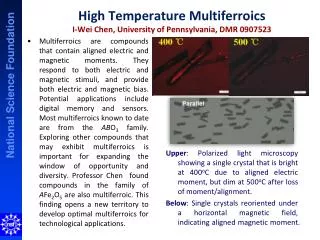
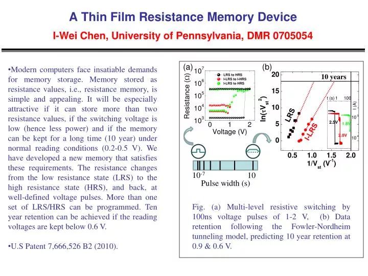
A Thin Film Resistance Memory Device I-Wei Chen, University of Pennsylvania, DMR 0705054. (a). (b).

E N D
A Thin Film Resistance Memory DeviceI-Wei Chen, University of Pennsylvania, DMR 0705054 (a) (b) • Modern computers face insatiable demands for memory storage. Memory stored as resistance values, i.e., resistance memory, is simple and appealing. It will be especially attractive if it can store more than two resistance values, if the switching voltage is low (hence less power) and if the memory can be kept for a long time (10 year) under normal reading conditions (0.2-0.5 V). We have developed a new memory that satisfies these requirements. The resistance changes from the low resistance state (LRS) to the high resistance state (HRS), and back, at well-defined voltage pulses. More than one set of LRS/HRS can be programmed. Ten year retention can be achieved if the reading voltages are kept below 0.6 V. • U.S Patent 7,666,526 B2 (2010). 10 years LRS I-LRS 10-7 10 Pulse width (s) Fig. (a) Multi-level resistive switching by 100ns voltage pulses of 1-2 V, (b) Data retention following the Fowler-Nordheim tunneling model, predicting 10 year retention at 0.9 & 0.6 V.
A Thin Film Resistance Memory DeviceI-Wei Chen, University of Pennsylvania, DMR 0705054 We have initiated a collaboration with Shanghai Institute of Ceramics, Chinese Academy of Sciences (host institute) to design improved thermoelectric materials which meet the unique requirement of high electrical conductivity and low thermal conductivity. Most materials are either good electrical and thermal conductors, like metals, or poor electrical and thermal conductors, like plastics, thus failing such requirements. Investigators from other US universities (Emory, Kansas, MIT) and industry (GM), and from Japan (Nagoya U) are also involved. Left is a workshop of these investigators in China in May, 2010. Please insert an image or group of images here to illustrate your broader impacts activities. If you need more space, you may reduce the adjacent textbox. Please use lettering that is clearly visible (i.e. not too small). Please include a brief figure caption.