Download
1 / 29
290 likes | 457 Views
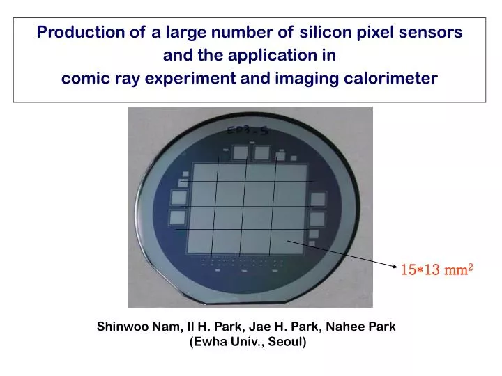
Production of a large number of silicon pixel sensors and the application in comic ray experiment and imaging calorimeter. 15*13 mm 2. Shinwoo Nam, Il H. Park, Jae H. Park, Nahee Park (Ewha Univ., Seoul). Two Applications. Cosmic Ray nuclei charge measurement by dE/dx For CREAM Experiment.

E N D
Production of a large number of silicon pixel sensors and the application in comic ray experiment and imaging calorimeter 15*13 mm2 Shinwoo Nam, Il H. Park, Jae H. Park, Nahee Park (Ewha Univ., Seoul)
Two Applications • Cosmic Ray nuclei charge measurement by dE/dx • For CREAM Experiment • Silicon Tungsten Calorimeter • For future ILC ECAL and Phenix NCC
Cosmic Rays All particle spectrum from direct and indirect cosmic ray observations Direct Measurement, Balloon, Satellite (< 1015 eV) ~ E-2.7 ~ E-3.0 Indirect Measurement, Air Shower (> 1015 eV) Taken from Simon Swordy http://hep.uchicago.edu/~swordy/crspec.html
Galactic component : Stochastic collision with moving magnetic clouds produced from Supernova Remnants accelerates comic rays. • Acceleration limit increases for high-Z nuclei.
∝ Charge Measurement of high energy particles (1012 - 1015 eV) • Energy loss of a charged particle in the matter by Bethe-Bloch formula • dE/dx : logarithmic dependence on particle energy • Radiative energy loss is small for proton and heavy nuclei
High Energy Particle current SiO2 P+ (0.6um) bias voltage Insulator : (1,1,1) 5 kΩ N-type N+ (1.0um) Al 82MeV Ni Silicon sensor for charge measurement • PIN diode operating at full depletion condition • Produced from wafers of 380 um, 5”, double polished Maximum signal (for 300 um thickness Si) 82 MeV / 3.62 eV ~ 2107 holes~> 3.20 pC
Charge detector Pixel Size of Sensors • CREAM is balloon borne experiment to measure cosmic composition in 1012 -1015 eV (highest possible energy range for a direct measurement) • Sensors are installed on top of the calorimeter and target • Back-scattered particles are produced in the high energy shower • Pixel size is to be optimized for the performance : 15*14 mm2 for CREAM Trigger Detector Charge Detector Calorimeter • Area to cover ~ 79 × 79 cm3 • Number of channel ~ 3000 for a layer -> 180 sensors
PIN diode structure Clean wafer Oxidation N+Diffusion Cover with photoresist Expose through mask Develop Etch, Stip P+ImplantationAnneal Metallization Fabrication process Sensor Fabrication Fabricated by SENS Technology (www.senstechnology.co.kr) Fabricated sensor Wafer size : 5 inch thickness: 380 um Pixel size : 1.55 × 1.37 cm2 Array : 4 × 4 matrix • Sawing / attach Kapton tape • for connection to readout • Kapton tape Cu wire with width 50 um • Wire (wedge) bonding • for connection of • Kapton cable to sensor pixel • Wedge bonding Al wire with diameter 50 um • Glob Top • for protection and preservation • of bond wire • Coating • SJC Polychemicals,DCE, DP100
Sensor Performance ~300 sensors for CREAM-1 (2003) ~400 sensors for CREAM-2 (2005) 1/C2 ILeakage Measurement Capacitance Measurement full depletion at ~ 80V Operation bias at 100V (over depletion) to make sure all sensors are fully depleted. • For most sensors leakage current below 10 nA/cm2 at full depletion voltage
Quality of Sensors Sensors are biased at 100V (Over-depletion Voltage) to make sure that all sensors are fully depleted with the variation in the thickness and resistivity
Analog Electronics (Frontend Readout) Frontend readout chip : CR1.4 16 pixels ADC CR1.4 ASIC • Custom VLSI (Very Large Scale Integrated circuit) chip • Developed for large arrays of silicon detectors in the Pamela experiment • 16 channels of charge inputs (integrating the charge pulses -> DC levels) • Multiplexed to common output line • Dynamic range : a few fC to about 9 pC with 1 mV/fC Gain, 1200 MIP • Power consumption : ≤ 6 mW/channel, ≤ 100 mW/chip • Noise ~ 5000 e- CR1.4 • 1 analog board = 7 CR1.4 * 16 channels = 112 channels
Silicon charge detector used in the second flight (2006.01, 28 days, Antarctica) • Total 4864 channels, 304 sensors • Sensitive area 779*795 cm2, No dead area between sensors • Consume power of 136W, Total 56kg, total height 100mm
SCD Assembly Mounting the assembled ladder Assembled SCD (1 layer) SCD cover SCD mechanical structure No damaged sensor was found after 28 days flight and parachute landing
Thermal solution sensors Analog board Thermal strap (aluminum 2mm) SCD radiator (sun-side) SCD radiator (anti sun-side)
Flight Monitoring Temperature was maintained below 37’C Pedestal runs were taken every 5 min. for offline correction
Channel Performance 95% of channels performed very well to see MIP. Rest 3.5% are good for high z events analysis. Pixels in y axis Pixels in x axis ADC counts (Proton signal is ~20 Counts above pedestal)
Calibration Data and Channel Uniformity • Helium events were taken with special trigger for calibration • Each sensor signal is well fit to Landau curve Distribution of Peak value of fit curve. RMS ~ 0.023 * Z
Charge Spectrum in the Flight Data p Very Preliminary He Very Preliminary O C Clean signals up to Fe Correlation between signals from top and bottom layers (Data are not corrected for detector acceptance) Mg Si Ne
Silicon-W imaging calorimeter for ILC Tungsten : small Moliere radius Sharp single particle shower Thin active layer with silicon Dean Karlen, LCWS 2002 Single particle showers from photons, neutral hadrons have to be well separated in a jet. For ILC Jets, about 26 GeV of photons have ECAL showers closer than 2.5 cmfrom a charged track Segmentation in Silicon sensors ~ 10 mm
Test module Assembly thickness : 3.5 mm (= 1 X0) Size 65.5 mm X 57.5 mm ( ~ sensor size) Tungsten Test Module : 20 layers stacked Frontend board Mount holes Aluminum Support of a Layer
Aluminum 1.5 mm Sensor and Readout 10 mm Tungsten 3.5 mm 15 mm Thickness of an Assembled Layer Connector 2.7 mm Capacitor 1.4 mm Pcb 1.7 mmResistor 0.65 mm Diode 1.15 mm CR 1.4 chip 2.45 mm Shielding board 1mm 1mm inactive gap between sensors Silicon Sensor 32 pixels in a layer 131mm X 115mm Frontend Board
Layers of Si sensors and Tungstens Digital and Control Boards Frontend readout boards Beam Direction
Test Module Setup Geometry • Total 20 layers = 20X with uniform layer thickness • Shower sampling at 19 layers with 2 sensors each layer. • 1mm gap between sensors • Aligned beam center to the center of a sensor 1mm inactive gap Effective RM :~ 45mm from volume ration of material RM 131mm X 115mm -> insufficient transverse shower containment
Channel Scan for MIP calibration Scanned over all 640 channels with 100 GeV hadron Beam (no tungsten) Pedestal : Gaussian Fit Mean : 5206.9 Sigma : 7.2 Signal : Landau Fit Peak : 5243 an example of a sensor with all good pixels S/N = 5.2 ADC Counts
Detector Response to Different Particles Random Trigger events (total pedestal) 50 GeV Electron Online Shower Profile Monitor Pedestal subtracted 50 GeV pion First Analysis : sum ADC counts of all channels No rejection of dead, noisy channels, No gain calibration applied 150 GeV Muon Total ADC of an event / 640
Detector Response to Different e- Energy Shower 150 GeV 100 GeV 80 GeV Readout Pedestals from Random Trigger 50 GeV 30 GeV 20 GeV 10 GeV Total ADC of an event / 640
Energy Resolution Preliminary • Geant4 simulation of this setup taking into account only shower leakage gives 18%/√E. • The effect of bad channels, gain calibration, and beam spread are not included here. • Working on further analysis Fit curve of 29%/√E dE / E (%) Electron Energy in GeV
New Silicon Sensors for ILC Si-W calorimeter (CALICE) Silicon thickness : 525 micronSize: Matrix of 6x6 pads, each pad have ~1cm2Nominal Bias 200V, leakage @ 200 V < 300 nA for the full matrixWafers passivationfor electrical contact with the glue EPOTEK E4-110 polytec (conductive glue with silver) 5” wafer 62mm pad ~1x1cm2 62mm 6*6 pixels CALICE main pattern
Design and production of a large number of silicon pixel sensors (more than 800) has been done. The sensor is 4*4 PIN diode array surrounded by 3 guard rings with each pixel size of 15*13 mm2, fabricated from 380 um high resistivity wafer. Most pixels have a low and stable level of leakage current (Id <10nA/cm2) at the operational bias of 100V. Sensors showed excellent performance in charge measurement of high-energy cosmic rays in balloon-borne experiment. The same sensors were successfully tested in high energy beam test for Si-W imaging calorimeter R&D. Summary