Download

1 / 36
380 likes | 565 Views
Electrical and Computer Department. Design and Test of Fault Tolerant Quantum Dot Cellular Automata. Outline. Introduction: QCA Technology Example QCA circuits Testing Majority Voter, Networks of MV DFT for QCA Novel Complex Universal Gate: AOI (And-OR-Inverter) Gate

E N D
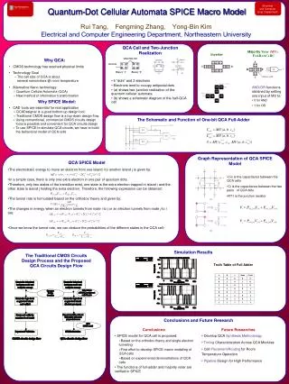
Electrical and Computer Department Design and Test of Fault Tolerant Quantum Dot Cellular Automata
Outline • Introduction: QCA Technology • Example QCA circuits • Testing Majority Voter, Networks of MV • DFT for QCA • Novel Complex Universal Gate: AOI (And-OR-Inverter) Gate • Synthesis with QCA technology • Future Research Directions
QCA Introduction(I) • Motivation • Approaching physical limits of CMOS sizing • Alternative technologies need to be investigated. • QCA as a nano scale solution • New method of computation and information transformation. • Current Manufacturing Status of QCA • Micro-sized QCA devices • latch and 2-bit shift register have been manufactured • Research focused on • molecular QCA devices for room temperature operation. • Initial analysis of a simple molecular systems reported.
QCA Introduction(II) • Speed* • @42 nm spacing: 25GHz • @4.2 nm spacing: 2.5THz • Clocking Zone Size* • assuming 5x20 cell zone size • In 42 nm: 0.16sq m • In 4.2 nm: 0.0016sq m • In 0.05 m CMOS: • Size of typical transistor = 0.56sq m • Top area of minimum wire contact =0.01sqm * In “Architectural Issues and Possibilities in Quantum Cellular Automata (QCA)” by M.T.Niemier and P.M.Kogge in NSF
QCA Cell QCA cell • QCA cell consisting of 4 “dots” and 2 extra electrons; • Information stored not as voltage level • Positions of electrons • Coulomb interaction between cells • No current in information transformation • Very low power dissipation. Rotated cells Quantum dot electron Binary ‘1’ Binary ‘0’
Cell Interaction QCA cell Binary Wire • Information is transferred by the Coulomb Interaction. Input Cell State Propagation Direction
QCA cell Basic QCA Devices Inverter A 1 0 B F 1 0 0 C Majority Voter: F=AB+AC+BC Coplanar Wire Crossing 1
Clock Field Strength Release Relax Switch Hold Clock Zone Phase State Propagation Direction 4-phase Clocking QCA cell • Timing in 4 time zones • 4 phases in each clock zone Zone 1 Zone 2 Zone 3 Zone 4
QCA Full Adder • The full adder consists of • 3 MVs • 2 Inverter • Different Shades of color represent clock zones
QCA Memory Cell • Memory stored in a loop. • Different Shades of color represent clock zones
Device cell Input A Input B Output F Input C A F B MV C Majority Voter (MV) • Implement logic AND/OR functions, by setting an input to: • 0 for AND, • 1 for OR gate. Output F as the majority of inputs: F=MV(A,B,C)=AB+AC+BC
A A B B Test Sets for MV • No built-in VDD or ground lines in QCA designs. • 2 extra inputs connected to logic “1” and logic “0” • Called control lines connected to one MV input • Implementing AND and OR logic functions. U1 U0 1 0 MV A MV A B B
Testing MV • 100% single stuck-at fault test set: • ABC= (010, 100, 101, 110) • Fault List: • A/1 (A stuck-at 1), A/0, B/1, B/0, C/1, C/0, d/1, d/0, Z/1, and Z/0 • 100% single stuck-at fault test set: • ABCU0U1= (11100, 00011) • Fault List: • A/0, B/0, C/0, d/0, and Z/0 • Additionally, • ABCU0U1 = (10011, 01100) • detects all faults on U0U1
U1 1 A g MV1 B i j MV3 C MV4 h Z MV5 D MV2 E F 0 U0 General Test Set for a Network of MVs • A logic network composed only of AND and OR gates • AND/OR implemented using QCA MVs. • 2 extra control inputs other than primary inputs: • U0,U1
General Test Set for a Network of MVs • Only 2 vectors needed to detect all SSFs • The 1st test vector • sets all primary inputs to “0” • sets 2 control inputs to “1” (all MVs OR gates) • detects all (multiple) stuck-at-1 faults • The 2nd test vector • sets all primary inputs to “1” • sets 2 control inputs to “0” (all MVs AND gates) • detects all (multiple) stuck-at-0 faults
General Test Set for a Network of MVs • Additional Vectors needed to detect faults in control lines (U0U1) • Conventional (combinational) ATPG tools used • MV replaced by a hierarchical cell implementing the majority function. • Network of MVs transformed into a hierarchical gate-level netlist. • Use ATPG for the pin faults on the control inputs
Testing NetworksAND, OR, INV • Universal Logic: AND, OR & INV • INVs prevent fault propagation by 2 test vectors A g • Without INV: • ABCDEFU0U1 = (00000011 • detects all stuck-at-1 faults • With INV: • ABCDEFU0U1 = (00000011) • cannot detect E/1 and F/1 • multiple faults masked • e.g. g/1 and E/1 B i1 i2 j C h Z D E F U1 1 A g MV1 B i2 i1 j MV3 C MV4 h Z MV5 D MV2 E F 0 U0
Control line U1 Inverting Block Non-Inverting Majority Voters Primary Inputs + Literals Primary Outputs Primary Inputs U0 Testing Networks of AND, OR & INV • Push all inversions to the primary input level. • An equivalent network of only AND and OR • take literals as inputs.
A B C Z D A B C U0 Z 0 D D A MV B MV C Z MV MV D D 1 U1 Pushing Back Inversions Push all inversion to the primary input MV implementation
QCA Manufacture Defects • Manufacture consists of Synthesis and Deposition • Defects in Synthesis part results in imperfect cells: • missing/extra dots; missing/extra electrons • Defects in Deposition part results in cell misplacement: • cell displacement, misalignment, etc. • Defect are much more likely to appear in the Deposition part * Personal correspondence with Prof. M. Lieberman in department of Chemistry and Biochemistry, University of Notre Dame
Fault model Majority Voter • Here we consider only cell misplacement faults caused in the deposition part. • Cell displacement: • defective cell is misplaced within original direction; • Cell misalignment: • direction of defective cell is misplaced; • Cell omission: • particular cell is missing compared to the defect-free design.
Synthesis Results Majority Voter • Synthesis tool: Synopsis Design Compiler and Synopsis Library Compiler • Synthesis results show that existing tools can not make efficient use of MV • Note: AND2 and OR2 can be implemented with MV
AOI (And-Or-Inverter) Gate • Motivation • MV is not universal, doesn’t have INV function • Not favorable for synthesis by existing tools • AOI gate • Universal complex gate, 7 cells • With embedded AND, OR and INV functions • Desirable for Synthesis • Arranged as two nested MVs
5nm 20nm 25nm 25nm 35nm 25nm 25nm 25nm Layout and Schematic AOI Gate • F=MV(D,E,MV(A’,B,C’)) • Two nested Majority Voters • Cell B has stronger effect on device than other input cells; • therefore placed further than other inputs D A B F MV1 MV2 D C A MV1 F B MV2 C E E
Wired AOI Gate AOI Gate A D • AOI gate is stable • Connect AOI gate to binary wire while preserving original logic function • Place wires apart to reduce interference 5nm 20nm 15 15 10 15 25nm B 25nm 15 15 35nm 15 15 25nm D 25nm A MV1 MV2 B C E C E
Properties AOI Gate Property 1. All input values are inverted output value is inverted; Property 2. Consider an arbitrary network of AOI gates with primary input vector V. If all bits are flipped, V V’,all nodes in network are flipped. Property 3. For any node in an arbitrary network of AOI gates, stuck-at-u fault is detected by input vector V stuck-at-u’ is detected by V’.
Logic Functions AOI Gate D A • AOI gate can be programmed into various 1-level and 2-level logic gates MV F B MV C E A=0 D=0 B=1 D=0 E=0 ORAND Gate NAND Gate (2-level) (1-level) B=1 D=0 A=0 D=1 E=0 NOTOR Gate NANDAND Gate (1-level) (2-level)
Synthesis Results(I) AOI Gate • Library consists of 8 two-level gates and 5 one-level gates derived from AOI gate • Area (# of cells) improvement compared to synthesis results using MV and INV
Synthesis Results(II) AOI Gate • Library Consists of 8 two-level gates and 5 one-level gates derived from the AOI gate • Gate count for each type of gates are shown • Area (# of cells) improvement compared to synthesis results using MV and INV are shown
D D A A 5nm 25nm 20nm • Fault-Free AOI Gate: • Cell size 20x20 sq.nm • Dot size 5nm • F=MV(MV(A’,B,C’),D,E) B 35nm Input Cell B Displacement Fault B 25nm 25nm 25nm 25nm 25nm 25nm 25nm 25nm 30nm 25nm C • Faulty AOI Gate: • F=MV(B,D,E) • Acts as a MV, • Cell A and C has no effect on output C E E Defect Characterization(I) AOI Gate
D A 5nm 20nm D Input Cell B Displacement Fault 10nm A • Fault-Free AOI Gate: • Cell size 20x20 sq.nm • Dot size 5nm • F=MV(MV(A’,B,C’),D,E) B 25nm 25nm 25nm 25nm 25nm 25nm 25nm 25nm 25nm 25nm • Faulty AOI Gate: • F=B • Output determined by horizontal input B alone B 35nm C E C Defect Characterization(II) AOI Gate
D 5nm A 20nm D Output Cell Displacement Fault A 15nm • Fault-Free AOI Gate: • Cell size 20x20 sq.nm • Dot size 5nm • F=MV(MV(A’,B,C’),D,E) 25nm 25nm 25nm 25nm B 30nm 25nm 25nm 25nm 25nm 25nm Faulty AOI Gate: F=D’E’+(D’+E’)(A’B+BC’+A’B’C’) B 35nm C C Defect Characterization(III) AOI Gate
Test Sets AOI Gate • Test set with 100% coverage to detect all cell displacement defects: • only 2 vectors needed • ABCDE={00000,00001} • Test set with 100% coverage to detect all PIN stuck-at faults: • 4 vectors needed • ABCDE={01110,00101,00000,00001} • Test sets generated using PIN fault model can cover all internal structural faults, very useful in test vector generation
A D AOI B F C E A D AOI B F C E Full Adder AOI Gate D Wired AOI gate • Full adder with MV, INV: • 3 MVs, 1 INV • 25 cells for active device A MV MV B F C E • Full adder with AOI: • 3 AOI gates • 14 cells for active device cout=a*b+b*cin+a*cin sum=a xor b xor cin a b cin
Future Research:Circuits • Establish Electrical Model for QCA • Design Sequential Modules in QCA • Delay Faults due to Defects (Kink Effect) • Interface Circuitry Between QCA and CMOS
Future Research: Systems • Develop QCA-Driven Synthesis • Timing Characterization Across QCA Modules • Cell Placement/Routing for Room Temperature Operation • Pipeline Design for High Performance