Download
1 / 32
330 likes | 728 Views
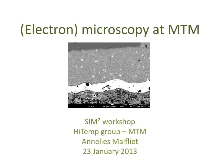
(Electron) microscopy at MTM. SIM² workshop HiTemp group – MTM Annelies Malfliet 23 January 2013. Content. Microscopy at MTM: in general Sample preparation In particular SEM XL30 FEG/XL40 LAB6 FEG-EPMA JXA-8530F TEM CM 200 FEG FEI Nova NanoSEM Contact details. Microscopy at MTM.

E N D
(Electron) microscopy at MTM SIM² workshop HiTemp group – MTM Annelies Malfliet 23 January 2013
Content • Microscopy at MTM: in general • Sample preparation • In particular • SEM XL30 FEG/XL40 LAB6 • FEG-EPMA JXA-8530F • TEM CM 200 FEG • FEI Nova NanoSEM • Contact details
Overview microscopy • https://www.mtm.kuleuven.be/English/Research/Equipment/List#_Microscopy New µscope FEI Nova NanoSEM
Core facility ‘Electron microscopy’ • State-of-the-art Scanning Electron Microscopy (SEM) and Transmission Electron Microscopy (TEM)
(Electron) microscopy’ • Imaging: phase distribution, particle size, topography, ... • Light Optical Microscopy (LOM) • Secondary Electron (SE) or Backscattered Electron (BSE) imaging (on SEM) • Bright-Field (BF) imaging (on TEM) • Chemical analysis: phase composition, presence of impurity elements, element distribution, ... • Energy Dispersive Spectroscopy (EDS) (on SEM/TEM) • Wavelength Dispersive Spectroscopy (WDS) (on FEG-EPMA) • Electron Energy Loss Spectroscopy (EELS) (on TEM) • Crystallography: crystal structure + texture • Electron Backscatterd Diffraction (EBSD) (on SEM) • Selected Area Electron Diffraction (SAED) or Convergent Beam Electron Diffraction (CBED) (on TEM) Broad spectrum of equipment and preparation facilities
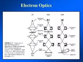
Electron microscopy • Difference LOM – EM • Source: light vs. electrons • Optical lenses vs. eletromagnetic lenses • Eye vs. Detectors • Resolution • Most used electron microscope is Scanning Electron Microscope (SEM)
SEM detectors • Typical detectors • Secondary electron detector (SE) • Good spatial resolution • Topography • Backscattered electron detector (BSE) • Strong atomic number contrast • X-ray detector • Elemental analysis • Different signals originate from different interaction volumes • Effect of voltage on interaction volume
Composition analysis • Based on emission of characteristic X-rays caused by excitation from eletron beam • X-ray can be detected by: • Energy Dispersive Spectroscopy • X-ray are separated based on their energy • Result is an energy-intensity spectron with peaks • Peak position identifies the element • Height ~ its concentration (standardless quantification) • Energy resolution ~127eV • Measuring time: 10-100s (all elements measured at the same time) • Wavelength Dispersive Spectroscopy • not on SEM, but on Electron Probe Micro Analysis (EPMA) • Higher spectral resolution • Typically quantification with standards • More time consuming (5 spectrometers up to 5 elements measured at the same time)
SEM - TEM • Difference SEM – TEM • Higher eV with TEM beam with smaller wavelength higher spatial resolution • Observe electrons passed through (and interacted with) the sample • Much smaller and especially thinner sample electron source D = 3 mm sample screen
Effort - information • Microscopy technique is mainly determined by • What information you would like to have • Size of the features of interest • Depending on technique, material and required sample ‘perfectness’, the parameters that determine effort are: • Sample preparation • Embedding: 15 min – 1 day curing/ conductive resin (under pressure) • Grinding/polishing: hard/brittle/porous/soluble in water(ethanol)/... • Conductive coating needed: thickness, homogeneity • Preventing contamination (air, moisture): storing in desiccator/vacuum/cryo cleaner/... • Removing contamination: plasma cleaner/... • Learning process • Training • Experience/practice! • Literature reading
Effort - information map • In general ...
Sample preparation at MTM • https://www.mtm.kuleuven.be/English/Research/Equipment/List#_Sample_preparation
Sample preparation grinding • In general: for LOM/SEM/EBSD (room 02.33) • Cutting • Ultrasonic cleaning: remove particles from pores • Embedding with • Technovit: cures very fast (15 min) • Epofix: better infiltrates pores better for powder or porous material (1 day curing under vacuum) • Predopress (pressure/hot mounting): harder resin better for harder materials (also conductive powder available for conductive resin no need for coating in case of conductive sample) • Grinding/polishing/OPS • Manual or automatic • Cooling + removing debris: water/ethanol/oil • OPS: soft/ductile materials • Different materials require different grinding + polishingprocedure best to talk with responsible technician polishing
Sample preparation • Especially for evaluation of interfaces or for soft material: Cross section ion polishing • Clean surface on large area (~ 1 mm²) • Disadvantage: more time consuming than mechanical polishing Au Ni-P Cu CP method Polishing time: 4 hours Mechanical polishing
Sample preparation • Etching (for metals) • In acid, electrolytically • Coating with C/Au/Pt/Au-Pd/Pt-Pd • Au-Pd: imaging surface topography/gives higher resolution • C: Chemical analysis, mapping, EBSD • Carbon rod: better suited for thin homogeneous layer than carbon wire • For EDS/WDS: Pay attention to overlap of peaks of coating and sample • Degassing in vacuum chamber Coating units at MTM
Sample preparation • TEM: more complicated + different methods depending on material • Separate TEM sample preparation room at MTM • Possible at MTM • Thin film: grinding/polishing/thinning/breakthrough (electrolytic,ion miller) • Replica method • Depositing on support grid • Ultramicrotome to cut slices • FIB • ...
SEM XL30 FEG • Equipment details • 0.2-30 kV • SE/BSE detector • EDS (detection from B) • Most frequent used EM • User-friendly • Many users • 1 day training • Reservation per 2 hour • 1-3 samples • Many users highly occupied (24h/d; 7d/w) • Alternative is SEM XL40 LaB6: • similar possibilities (SE/BSE, EDS, ...) • Particle analysis software • LaB6 vs. FEG: LaB6 has larger probe diameter and less brightness, but for many applications it can be sufficient • Almost not used XL30: BSE image + EDS analysis XL40: BSE image
Main features • In-Lens Schottky Field Emission Gun (FEG) • 1 - 30 kV, 50 pA – 500 nA, 40 nm minimum probe size • Imaging • Electron detectors: SE + BSE • 40x to 300,000x magnification • Cathodeluminescence system • Monochromatic + panchromatic • Phase composition • EDS system: Resolution: 129 eV @ MnKa • WDS system: 5 full scanner type X-ray spectrometers
FEG-EPMA: Use • Typical analysis type • Composition quantification using standards • Including minor and light elements • Mapping elemental distribution • Better spectral resolution oxidation state of elements • 0.5-1 day/sample • Possible to let it run overnight by setting measurement points or mapping area • 3-day training • Users are through promotors of the FEG-EPMA • For external and occasional measurements, technical responsible at MTM can do the measurement
TEM CM 200 FEG • Details • 20-200 kV • Resolution < nm • EDS/EELS • GATAN Tridiem Image Filter • Few users • Several day training
TEM: Use • Characterization of nanoscale particles with respect to their shape, size, structure, chemical composition and distribution. • Imaging • Diffraction: crystal structure • Composition analysis • EDS • EELS: especially useful for light elements
FEI Nova Nanosem • FEI Nova Nanosem • Imaging (SEM with TLD) • High resolution • Low keV imaging • ‘Pure’ samples (not coated) • Difficult samples (magnetic, non-conductive) • Chemical analysis (EDS) • Phase/ texture analysis (EBSD) • Chrystallographic characterisation • Integration with EDS phase analysis • Plasmacleaner • Just installed, about to be operational Anodized Ti EDS+EBSD
What if you would like to use one of the microscopes at MTM?
Contact details • For more information: • Core facility Electron microscopy: Tom Van der Donck (tom.vanderdonck@mtm.kuleuven.be) • SEM XL30/XL40: Rudy De Vos (rudy.devos@mtm.kuleuven.be) • Annelies.malfliet@mtm.kuleuven.be • If you are advised to have a training, use the training request form available at https://ppms.info/kuleuven/treq/?pf=2