Download
1 / 25
250 likes | 427 Views
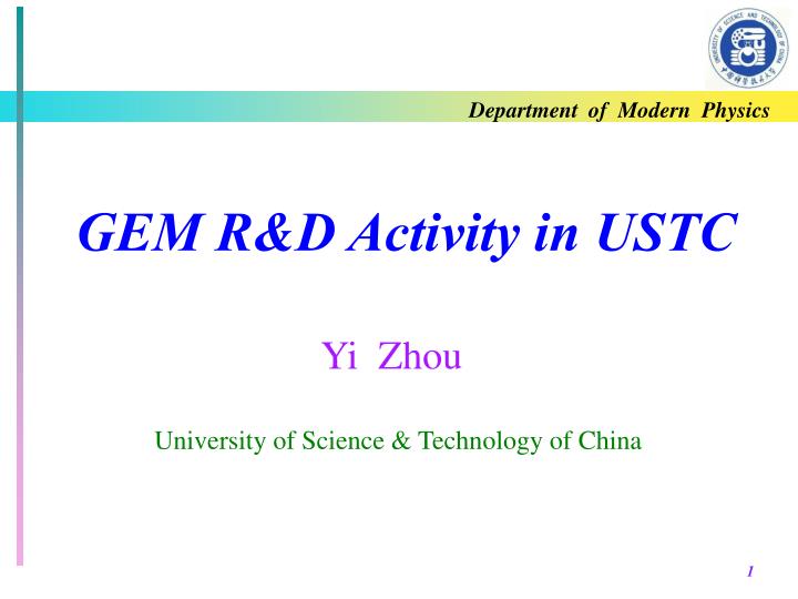
GEM R&D Activity in USTC. Yi Zhou. University of Science & Technology of China. Outline. GEM C hamber Design and Test Delay-Line Readout Method. Structures of GEM. 80 µm. Cu 5µm. Kapton 50µm. 60µm. 140 μm. GEM Chamber Design and Test Double-Layer Chamber 55 Fe Test

E N D
GEM R&D Activity in USTC Yi Zhou University of Science & Technology of China
Outline • GEMChamberDesign and Test • Delay-Line Readout Method
Structures of GEM 80µm Cu 5µm Kapton 50µm 60µm 140 μm
GEMChamberDesign and Test Double-Layer Chamber 55FeTest Energy Resolution-HV Gain-HV 2.Position Resolution(8keV X-ray Imaging)
Double-GEM DetectorDesign Two orthogonal sets of parallel strips at 0.8 mm pitch, 0.35 mm wide on upper side, 0.65 mm wide on lower side. The thickness of the PCB is 0.2mm
Effective Gas Gain 1 ( 70%Ar+30%CO2 )
Effective Gas Gain 2 ( 60%Ar+40%CO2 )
HV Optimization P2 P1 GEM1=420V GEM2=370V P2 GEM1=370V GEM2=420V ( 70%Ar+30%CO2 ) P1 While the effective gas gain is large enough, higher 1st GEM HV and lower 2nd GEM HV will give a better energy resolution.
Count ability and stability • Test time:~2 weeks; • Effective gain varied: <1%。 • Facula area of X-ray: 2mm2; • Counted by a scaler
X-rayImaging Experiment X: 6 readout channels Y: 6 readout channels 8-channel charge sensitive pre-amplifier × 2 Sensitivity: 0.8V/pc, designed by HEPG
Why Delay-Line? • Channel by Channel readout electronics cost too much; • The readout electronics based on integrated chip will be available soon (in China), but not now; • Delay-Line readout method can be used for low-rate application and the cost is much lower, the position resolution is not bad.
Delay-line Readout Method TheDelay-Line circuit is a chain of Inductor-Capacitor (LC) cells, an ideal LC cell could delay the input signal for a certain period with very small distortion. • Parameters of Delay-Line:
The Delay-Line PCB Department of Modern Physics
Simulation of the Delay-Line System Department of Modern Physics
Simulation and Calibration Signals Simulation: 1.38ns/cell Experiment: 1.41ns/cell
2D Images COG imaging σx~148.4μm σy~157.0μm
2D Images COG imaging σx~148.4μm σy~157.0μm
Summary & Outlook • A detailed test of gain & energy resolution for the double GEM detector has been performed; The energy resolution can be optimized by change the HV distribution while the gas gain is fixed. • Two readout methods have been studied; The channel by channel (COG) readout method has a good position resolution but costs too much. The delay-line readout costs low, when its position resolution can be accepted, it is a good choice for low-rate application. • Construct a prototype of a large area GEM; • Structure and HV optimization; • Readout PCB design. Thank You