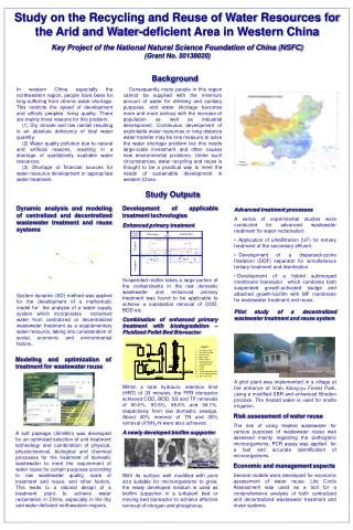
Download
1 / 14
140 likes | 258 Views
Case Study: Simultaneous Switching Outputs (SSOs). SSO Case Study. Device : RT54SX72S Output Bus: 32 bits Method: Divided into 4 banks of 8 SSOs, each bank enabled using BUFDs for staggering Analyzed for worst-case:

E N D
SSO Case Study • Device : RT54SX72S • Output Bus: 32 bits • Method: • Divided into 4 banks of 8 SSOs, each bank enabled using BUFDs for staggering • Analyzed for worst-case: • SSO mitigation (ΔT between banks for fast process and speed grade/cold/high voltage) • Setup time limitations (ΔT between first and last output enabling for slow process and speed grade/hot/low voltage)
RT54SX72S 47 rows 126 columns
Case A • All macros auto-placed by Designer • No manual adjustments to placement Outputs Enable Path
Case A: Auto-placement Max ΔT Min ΔT • Minimum ΔT between banks: ~ 3 ns • Maximum ΔT between 1st and last output enabling: ~ 25 ns (average 7ns per stage)
Case B • All macros initially auto-placed by Designer • Subsequently, BUFDs are placed manually to achieve significant increase in delays due to routing • Each pair of [logically] adjacent BUFDs separated by ~40 rows and ~40 columns Outputs Enable Path
Max ΔT Min ΔT Case B: 40 x 40 Separation • Minimum ΔT between banks: ~ 6 ns • Maximum ΔT between 1st and last output enabling: ~ 46 ns (average 14 ns per stage)
Case C • Modification of Case B with smaller separation distance between BUFDs • Each pair of [logically] adjacent BUFDs separated by ~15 rows and ~15 columns Outputs Enable Path
Case C: 15 x 15 Separation Max ΔT Min ΔT • Minimum ΔT between banks: ~ 4 ns • Maximum ΔT between 1st and last output enabling: ~ 37 ns (average 8 ns per stage)
Case D • All output macros are hand-placed together along one side of the die • Provides for “convenient” (seemingly optimal) board layout • All other macros are auto-placed Outputs Enable Path
Case D: “Pretty” Layout Max ΔT Min ΔT • Minimum ΔT between banks: ~ 1 ns • Maximum ΔT between 1st and last output enabling: ~ 11 ns (average 4 ns per stage)
Delay Summary Method Spacing Range A: Auto-placement 3 25 B: 40 x 40 Separation 6 46 C: 15 x 15 Separation 4 37 D: “Pretty” Layout 1 11