Download
1 / 38
430 likes | 609 Views
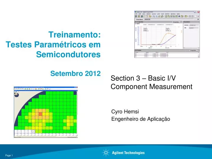
Treinamento : Testes Paramétricos em Semicondutores Setembro 2012. Cyro Hemsi Engenheiro de Aplicação. Section 3 – Basic I/V Component Measurement. Agenda. Section #3 – Basic I/V Component Measurement Making Accurate Resistance Measurements Characterizing Diodes & Transistors.

E N D
Treinamento:Testes ParamétricosemSemicondutoresSetembro 2012 Cyro Hemsi Engenheiro de Aplicação Section 3 – Basic I/V Component Measurement
Agenda • Section #3 – Basic I/V Component Measurement • Making Accurate Resistance Measurements • Characterizing Diodes & Transistors
- V + I d L W Understanding Resistivity and Resistance When characterizing materials we typically want to know the resistivity, which is a material property that is independent of the dimensions of the device being measured.
Rs Rs = Understanding “Ohms per Square” You may sometimes see the term “Ohms per Square”. This is simply another way of specifying resistivity. As long as the thickness of a material is constant, it has the same measured resistance for any sized square of the material.
Van derPauw Structures are Typically Used to Measure Resistivity On-Wafer Note that these structures are inherently designed to be measured using Kelvin measurements. - Kelvin measurement technique for surface resistivity ρmeasurement
Measuring Resistance: A Trivial Measurement? V = I x R, correct? NO! V = I x R(T) Resistance depends on temperature! This is referred to as the Joule self-heating effect. Resistance measurement is a tricky balance between two factors: To keep the resistor from heating up and the resistance value from changing, we need to keep the current (= power) low. Small currents imply that we need to measure smaller voltages, which in-turn requires more voltage measurement resolution capability.
The Importance of Thermal Resistance - We cannot arbitrarily increase the power (= current) into a Resistor to compensate for insufficient accuracy measurement hardware SiO2 h SiO2 0.014 W/oC-cm2 SiO2 thermal conductivity 1 cm 1 cm (h ´ 71) oC-cm2/W, or 0.007 oC-cm2/W for h = 1 mm SiO2 thermal resistance max power dissipation • For a 1 cm2 block of SiO2 1 mm thick, if you apply 1 W the temperature will rise by 0.007 oC • For a 10 mm2 block of SiO2 1 mm thick, if you apply 1 W the temperature will rise by 7,000 oC!
How Much Power Can I Apply to a Structure? Voltage resolution Max power dissipation At or near room temperature the resistance of a Cu or Al metal line changes by about 0.35%/oC. This allows us to compute the maximum amount of power that can be dissipated to produce a 0.1% change in resistance for a Cu or Al metal square 10 mm by 10 mm. To achieve 0.1% accuracy in a copper structure with an equivalent resistance of 10 mW per square (1 mm thick film) we have the following: Need 1 mV of voltage measurement resolution!
R = (VM1 – VM2)/IF Force Current Twice (Both Ways), i.e. +/- IF R 0 V VOFF1 VOFF2 + + + + SMU 1 SMU 2 VM1 V - - - - VEMF*1 VEMF2 VMU 1 (SMU 3) VMU 2 (SMU 4) VM2 VM1 VMU 2 (SMU 4) VMU 1 (SMU 3) Modified Kelvin Resistance Measurement • Key Points: • Make sure that you eliminate Joule self-heating effects • Measure twice and average the two resistances • measure the resistance twice • using the Kelvin measurement technique • reversing the polarity of the force current * transient voltage pulse created when reed relay switches open and close
Quick Review of Semiconductor Theory “Abrupt” Semiconductor Junction: Holes and electrons flow into the n and p regions (respectively) until the force of diffusion is exactly balanced by the electric field created by the fixed charge. Ex: “p- and n- doped” silicon electric field created by the fixed charges
Semiconductor Current Flow Equations The one-dimensional (x-axis) equations defining current flow in a semiconductor are shown below. Where J is the current density of electrons (n) and holes (p) q is the electron charge Ex is the electric field in the x-dimension m is the mobility of electrons (n) and holes (p) D is the diffusion constant for electrons (n) and holes (p) n is the electron density p is the hole density Current flow in a semiconductor consists of two parts: - a drift current proportional to the applied electric field and - a diffusion current proportional to the spatial first derivative of the free carrier density.
Einstein Relationships Link Mobility and Diffusion Constants The Einstein relationship relates the ratios of the mobility and diffusion constants as shown below. Where q is the magnitude of the electron charge (1.602 ´ 10-19 Coulomb) k is Boltzmann’s constant (1.38 ´ 10-23 J/K) T is the absolute temperature [deg K] m is the mobility of electrons (n) and holes (p) D is the diffusion constant for electrons (n) and holes (p)
Poisson’s Equation The general form of Poisson’s equation relates the second derivative of the electric potential to the total space charge density (r). Since we know that in a semiconductor this has to be related to the densities of mobile and fixed charge, we can write this as follows. Where Nd is the donor density concentration (dopation) Na is the acceptor density concentration eSi is the permittivity of silicon Space chargedensity electric potential The depletion approximation assumes that the semiconductor is divided into distinct regions which are either completely neutral or completely depleted of mobile carriers. This allows us to re-write the above equation as: abrupt junction
The Electric Field in a PN Junction We can integrate Poisson’s equation to get the electric field in both the p and n regions as shown below. Where xp is the width of the space charge in the p region xn is the width of the space charge in the n region Graphically, these equations have the appearance shown on the right. Electric field in both the p and n regions
Dopant Concentration & Space Charge Region We know that the electric field has to be continuous at x = 0. This gives us the result shown below. This equation shows an important characteristic of pn junctions: the width of the depletion region varies inversely with the magnitude of the dopant concentration. In other words, higher dopant concentrations result in narrower space charge regions. Dopant concentration Depletion region width
Semiconductor Diode Equation 1) When no voltage is applied to the pn junction a barrier exists to current flow. 2) As we apply a positive voltage to the p-region we reduce the built-in electric field of the pn junction. 3) At some point the electric field is reduced enough to allow current to flow .
Diode Characterization - 1 A forward diode characterization plotting both Id (blue) and log Id (orange).
Diode Characterization - 2 The reverse breakdown characteristics of a diode.
Review of MOSFET Operation - 1 Here we assume that the voltage applied to the drain (Vd) is small relative to the gate voltage (Vg) . The current is defined by the charge in the channel divided by the transit time: Highly doped channel Voltage to invert the channel Vg creates a conductive channel Where mn is the electron mobility W is the channel width L is the channel length Cox is the capacitance per unit area in accumulation
Review of MOSFET Operation - 2 As Vd increases it is no longer negligible relative to Vg, and the space charge region looks like a trapezoid. We make the approximation that the average channel voltage is Vg – Vd/2.
Review of MOSFET Operation - 3 If we plot out the previous equation for different values of Vd, then we get a family of parabolas: Vg However, the slope of the curves for Vd > Vg - Vt is negative and this does not make any physical sense as it would correspond to a negative transconductance.
Review of MOSFET Operation - 4 When Vd becomes greater than (Vg - Vt) the inversion layer becomes pinched off at the drain. However, as the electrons approach the drain there is no barrier to stop them and they are rapidly accelerated by the high electric field into the drain region. In this situation the current is determined by the rate at which electrons reach the edge of the depletion region, which is in-turn determined by the maximum electron drift velocity. Since the maximum drift velocity is (at least to first order) insensitive to Vd, once Vd reaches the value of (Vg - Vt) the drain current becomes saturated (constant).
Review of MOSFET Operation - 5 In saturation, the drain current is given by the equation shown on the right.
Review of MOSFET Operation - 6 The constants shown in the equation on the previous slide are usually combined into a single constant, beta: In the case where the transistor source terminal is not at ground it is a correct assumption that (at least to first order) an increase in Vs will have the effect of reducing the influence of the gate voltage. Therefore, it is reasonable to modify the equation for Id in saturation for the case where Vs ¹ 0 as follows:
MOSFET Vt Characterization Vt Extrapolating a plot of the square root of Id back to the x-axis is one way of determining the transistor Vt.
Non-Zero Bulk Voltage - 1 Applying a negative charge on the bulk will induce positive charge to accumulate near the bulk contact. This causes Vt to increase with decreasing values of Vb (which is commonly known as the “body effect”). Similarly, applying a positive charge on the bulk will cause Vt to decrease.
Non-Zero Bulk Voltage - 2 Negative values of Vb shift the curve to right which implies an increase in the threshold voltage (Vt). Similarly, positive values of Vb shift the curve to the left which implies a decrease in the threshold voltage.
Review of Bipolar Transistor Operation - 1 Consider the case where we have the emitter of the NPN transistor at ground and we apply a positive voltage to the base. We are also assuming the transistor collector is at a voltage much greater than that of the base (VC >> VB). If the base to emitter voltage (VBE) is sufficiently large enough to forward bias the base to emitter junction, then current will flow in the transistor as shown below.
Review of Bipolar Transistor Operation - 2 As can be seen from this equation, the base to emitter voltage does not need to change much in order to have large changes in the collector current. Therefore, once the NPN transistor has a sufficiently large VBE to become actively biased the magnitude of the collector current is limited by the amount of current entering into the base of the transistor.
Bipolar Characterization – Gummel Plot (1) A Gummel plot is usually used to determine the value of beta for various values of collector current. One method to perform a Gummel plot on an NPN transistor is to set the collector and base to zero volts and to sweep the emitter negatively. The values of base current and collector current are then measured and plotted on a log scale
Bipolar Characterization – Gummel Plot (2) As this plot shows, the value of the transistor beta is actually dependent upon the large-signal value of the collector current, although it is approximately constant over a fairly wide range of collector current values.
Bipolar Characterization – Emitter Resistance (1) The flyback method is the most common means used to determine Re. The SMU connected to the collector terminal is placed in current force mode with a very small force value (almost zero amps), making it essentially a high-impedance voltmeter. The SMU connected to the base terminal is also set to current force mode and the collector-emitter voltage (Vce) is measured and plotted versus the base current (Ib).
Bipolar Characterization – Emitter Resistance (2) The slope of the line in the flyback region can be determined by creating a regression line at predefined points using the built-in EasyEXPERT analysis functions. The slope of this line is in units of amps/volt; this is the inverse of resistance (which has units of volts/amp). Therefore, the inverse of the regression line slope gives us the value of emitter resistance (Re).
Power Bipolar Transistor Breakdown Characterization using the B1505A (1) As in the case of power MOSFETs, the breakdown voltages of power bipolar devices are also very important parameters. The junction breakdown voltages of power BJTs are defined as follows. BVcbo – The collector-base breakdown voltage with the emitter open BVceo – The collector-emitter breakdown voltage with the base open BVebo – The emitter-base breakdown voltage with the collector open
Power Bipolar Transistor Breakdown Characterization using the B1505A (2)