Download
1 / 8
100 likes | 379 Views
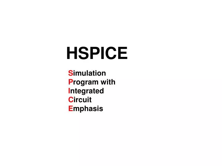
HSPICE. S imulation P rogram with I ntegrated C ircuit E mphasis. filename .protect .lib 'D:modeltsmcMIXED035mm0355v.l ' TT .unprotect .op .options nomod post VDD 1 0 3.3v R1 1 2 0. 1k V2 2 0 0v .param W1=5u M1 2 3 0 0

E N D
HSPICE Simulation Program with Integrated Circuit Emphasis
filename .protect .lib 'D:\model\tsmc\MIXED035\mm0355v.l ' TT .unprotect .op .options nomod post VDD 1 0 3.3v R1 1 2 0.1k V2 2 0 0v .param W1=5u M1 2 3 0 0 +nch L=0.35u W='W1' m=1 +AD='0.95u*W1' PD='2*(0.95u+W1)' +AS='0.95u*W1' PS='2*(0.95u+W1)' VGS 3 0 0v .DC V2 0 3.3v 0.1v SWEEP VGS 0.1v 3v 0.25v .alter .param r1=10k .alter .param r1=100k .alter .param r1=10000k .PROBE I(R1) I(M1) .end File name TSMC model List All Terminal’s Voltage Require to obtain graphical result for Avanwave. Body Drain Define W1 = 5u Source AD, AS : the area of the source , drain region(optional) PS, PD : the peripheral length of source, drain region Gate Type Return Simulation with Different Parameter Values
Website : http://alg.csie.ncnu.edu.tw/~csou/
Homework 1 d9662836 資工系 歐家欣
1 1_1 3 2
Code PMOS .protect .lib 'D:\model\tsmc\MIXED035\mm0355v.l' TT .unprotect .op VDD 1 0 3.3v R1 2 0 100k Rsd 1 1_1 0K V2 2 0 0v M1 2 3 1_1 1_1 +pch L=0.35u W=5u m=1 VG 3 0 0v .DC V2 0 3.3v 0.1v SWEEP VG 0.1v 3v 0.25v .PROBE I(Rsd) .end