Download
1 / 15
150 likes | 238 Views
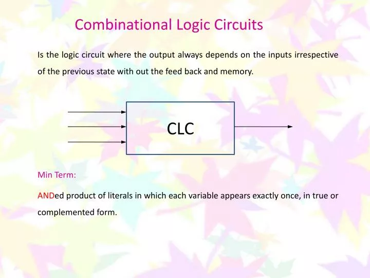
Combinational Logic Circuits. Is the logic circuit where the output always depends on the inputs irrespective of the previous state with out the feed back and memory. CLC. Min Term:. AND ed product of literals in which each variable appears exactly once, in true or complemented form.

E N D
Combinational Logic Circuits Is the logic circuit where the output always depends on the inputs irrespective of the previous state with out the feed back and memory. CLC Min Term: ANDed product of literals in which each variable appears exactly once, in true or complemented form.
Canonical Forms One of the most powerful theorems within Boolean algebra states that any Boolean function can be expressed as the Sum Of Products (SOP) of all the variables with in the system . A+B = A(1)+B(1) = A(B+B’)+B(A+A’) = AB+AB’+AB+A’B Min Terms F in canonical form: F(A,B,C) = Sm(3,4,5,6,7) = m3 + m4 + m5 + m6 + m7 = A' B C+A B' C’+A B' C+A B C’+A B C
Product of Sums (POS) ORed sum of literals in which each variable appears exactly once in either true or complemented form, but not both. F(A,B,C) = P M(0,1,2) = (A + B + C) (A + B + C') (A + B' + C) Maxterms
Finding the Minterms • Write down all the terms • Put X’s where letters must be provided to convert the term to a min term. • Use all combinations of the X’s in each term to generate minterms, where • an X is a 0, write barred letter; where it is 1, write an unbarred letter. • D. Drop out redundant terms. Example: Find the minterms for A+BC =A+BC =AXX+XBC (A00,A01,A10,A11 + 0BC,1BC) AXX= AB’C’, AB’C, ABC’, ABC XBC=A’BC, ABC = AB’C’+ AB’C+ ABC’+ ABC+A’BC+ ABC = AB’C’+ AB’C+ ABC’+ ABC+A’BC
Minterm Designation Example: find the minterm designation of AB’C’D’ Copy the term AB’C’D’ Substitute 1 for non barred 1 0 0 0 And 0 for barred letters Express as decimal subscript of m m8 Therefore, AB’C’D’= m8 So the answer of the last Example can be written as, AB’C’+ AB’C+ ABC’+ ABC+A’BC = Σm(4,5,6,7,3)
Minimization Technique Logic Minimization: reduce complexity of the gate level implementation • reduce number of literals (gate inputs) • reduce number of gates • reduce number of levels of gates • KARNAUGH MAP (K-Map) • TABULATION METHOD • (Quine-McCluskey Method)
Karnaugh Map Method K-map is a method of representing the truth table that helps to visualize adjacencies in up to 6 dimensions 2-variable K-map 3-variable K-map 4-variable K-map
Example: Reduce the expression F = Σm(0,1,2,3,6,7,13,15) by mapping and implement in NAND logic. • Enter 1 for given minterms in corresponding location and 0 for others. • Group the maximum number of 1s in the order of 2n. • Ensure that all the 1s must come under at least once in a group. • Simplify the resultant minterms using basic laws and OR the Result. • Implement the hardware. CD 00 01 11 10 AB Group I = A’B’C’D’A’B’C’DA’B’CD A’B’CD’ = A’B’ 00 01 11 10 Group II = A’BCDA’BCD’A’B’CD A’B’CD’ = A’C 0 0 Group III = ABC’DABCD = ABD 0 0 0 F = A’B’+A’C+ABD 0 0 0
NAND Implementation A’ B’ F = A’B’+A’C+ABD A’ C A B D
Å = + X Y X Y X Y Half Adder Sum = X’Y+XY’ = XY Carry = XY XOR XNOR Å = + X Y X Y X Y
Full Adder SUM= Carry Out=
I0I1I2I3I4I5I6I7 8:1mux Z I0I1I2I3 4:1mux Z I0I1 2:1mux Z A B C A B A Multiplexers / Data Selectors • 2n data inputs, n control inputs (called "select line"), 1 output • Used to connect 2n points to a single point • Control signal pattern forms binary index of input connected to output 2:1 mux: Z = A' I0 + A I1 4:1 mux: Z = A' B' I0 + A' B I1 + A B' I2 + A B I3 8:1 mux: Z = A'B'C'I0 + A'B'CI1 + A'BC'I2 + A'BCI3 +AB'C'I4 + AB'CI5 + ABC'I6 + ABCI7 In general, Z = (mkIk)
G O0 S O1 G O0 O1 O2 O3 S1 S0 Demultiplexers /Decoders • Single data input, n control inputs, 2n outputs • Control inputs (called “selects” (S)) represent binary index of output to which the input is connected • Data input usually called “enable” (G) 2:4 Decoder 1:2 Decoder 2:4 Decoder O0 = G S1’ S0’ O1 = G S1’ S0 O2 = G S1 S0’ O3 = G S1 S0 1:2 Decoder O0 = G S’ O1 = G S
Flip Flops Bistable Multivibrator • RS Latch • Reset-Set (RS) Flip Flop • J-K Flip Flop • Toggle (T) Flip Flop • Data Storage (D) Flip Flop