Download
1 / 13
140 likes | 520 Views
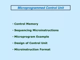
Microinstruction : Control Word in Control MemoryThe microinstruction specifies one or more microoperations MicroprogramA sequence of microinstructionDynamic microprogramming : Control Memory = RAMRAM can be used for writing (to change a writable control memory) Microprogram is loaded initiall

E N D
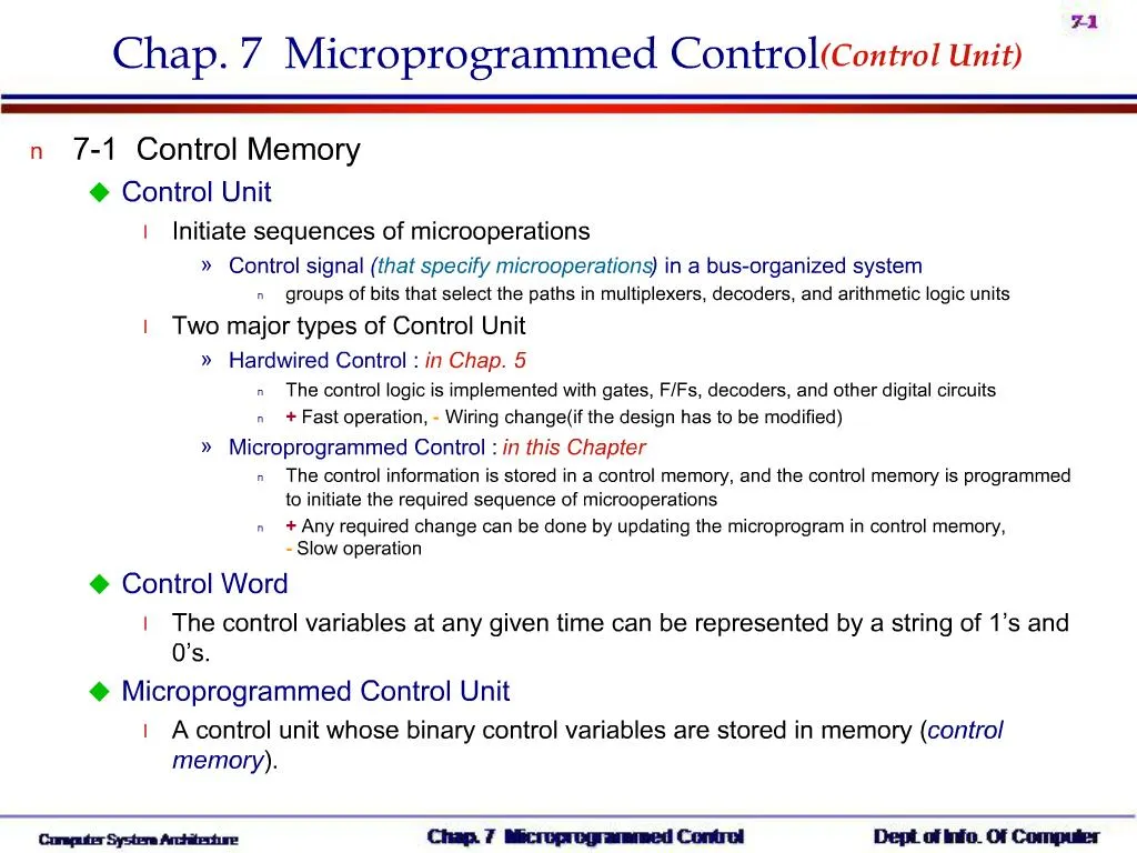
1. Chap. 7 Microprogrammed Control(Control Unit) 7-1 Control Memory
Control Unit
Initiate sequences of microoperations
Control signal (that specify microoperations) in a bus-organized system
groups of bits that select the paths in multiplexers, decoders, and arithmetic logic units
Two major types of Control Unit
Hardwired Control : in Chap. 5
The control logic is implemented with gates, F/Fs, decoders, and other digital circuits
+ Fast operation, - Wiring change(if the design has to be modified)
Microprogrammed Control : in this Chapter
The control information is stored in a control memory, and the control memory is programmed to initiate the required sequence of microoperations
+ Any required change can be done by updating the microprogram in control memory, - Slow operation
Control Word
The control variables at any given time can be represented by a string of 1�s and 0�s.
Microprogrammed Control Unit
A control unit whose binary control variables are stored in memory (control memory).
2. Microinstruction : Control Word in Control Memory
The microinstruction specifies one or more microoperations
Microprogram
A sequence of microinstruction
Dynamic microprogramming : Control Memory = RAM
RAM can be used for writing (to change a writable control memory)
Microprogram is loaded initially from an auxiliary memory such as a magnetic disk
Static microprogramming : Control Memory = ROM
Control words in ROM are made permanent during the hardware production.
Microprogrammed control Organization : Fig. 7-1
1) Control Memory
A memory is part of a control unit : Microprogram? ???? ??
Computer Memory (employs a microprogrammed control unit)
Main Memory : for storing user program (Machine instruction/data)
Control Memory : for storing microprogram (Microinstruction)
2) Control Address Register
Specify the address of the microinstruction
3) Sequencer (= Next Address Generator)
Determine the address sequence that is read from control memory
Next address of the next microinstruction can be specified several way depending on the sequencer input : p. 217, [1, 2, 3, and 4]
3. 4) Control Data Register (= Pipeline Register )
Hold the microinstruction read from control memory
Allows the execution of the microoperations specified by the control word simultaneously with the generation of the next microinstruction
RISC Architecture Concept
RISC(Reduced Instruction Set Computer) system use hardwired control rather than microprogrammed control : Sec. 8-8
7-2 Address Sequencing
Address Sequencing = Sequencer : Next Address Generator
Selection of address for control memory
Routine
Microinstruction are stored in control memory in groups
Mapping
Instruction Code Address in control memory(where routine is located)
Address Sequencing Capabilities : control memory address
1) Incrementing of the control address register
2) Unconditional branch or conditional branch, depending on status bit conditions
3) Mapping process ( bits of the instruction address for control memory )
4) A facility for subroutine return
4. Selection of address for control memory : Fig. 7-2
Multiplexer
? CAR Increment
? JMP/CALL
? Mapping
? Subroutine Return
CAR : Control Address Register
CAR receive the address from
4 different paths
1) Incrementer
2) Branch address from
control memory
3) Mapping Logic
4) SBR : Subroutine Register
SBR : Subroutine Register
Return Address can not be stored
in ROM
Return Address for a subroutine is
stored in SBR
5. Conditional Branching
Status Bits
Control the conditional branch decisions generated in the Branch Logic
Branch Logic
Test the specified condition and Branch to the indicated address if the condition is met ; otherwise, the control address register is just incremented.
Status Bit Test ? Branch Logic? ?? ?? : Fig. 7-8
4 X 1 Mux ? Input Logic(Tab. 7-4)?? ??
Mapping of Instruction : Fig. 7-3
4 bit Opcode = specify up to 16 distinct instruction
Mapping Process : Converts the 4-bit Opcode to a 7-bit control memory address
1) Place a �0� in the most significant bit of the address
2) Transfer 4-bit Operation code bits
3) Clear the two least significant bits of the CAR (?, 4 ?? Microinstruction ?? ??)
Mapping Function : Implemented by Mapping ROM or PLD
Control Memory Size : 128 words (= 27)
6. Subroutine
Subroutines are programs that are used by other routines
Subroutine can be called from any point within the main body of the microprogram
Microinstructions can be saved by subroutines that use common section of microcode
??) Memory Reference ???? Operand? Effective Address? ??? Subroutine
p. 228, Tab. 7-2?? INDRCT (???? FETCH? INDRCT? Subroutine)
Subroutine? ORG 64, ? 1000000 - 1111111? ??(Routine? 0000000 - 0111111)
Subroutine must have a provision for
storing the return address during a subroutine call
restoring the address during a subroutine return
Last-In First Out(LIFO) Register Stack : Sec. 8-7
7-3 Microprogram Example
Computer Configuration : Fig. 7-4
2 Memory : Main memory(instruction/data), Control memory(microprogram)
Data written to memory come from DR, and Data read from memory can go only to DR
4 CPU Register and ALU : DR, AR, PC, AC, ALU
DR can receive information from AC, PC, or Memory (selected by MUX)
AR can receive information from PC or DR (selected by MUX)
PC can receive information only from AR
ALU performs microoperation with data from AC and DR (??? AC? ??)
2 Control Unit Register : SBR, CAR
7. Instruction Format
Instruction Format : Fig. 7-5(a)
I : 1 bit for indirect addressing
Opcode : 4 bit operation code
Address : 11 bit address for system memory
Computer Instruction : Fig. 7-5(b)
16 ???? ???? 4 ?? ??
Microinstruction Format : Fig. 7-6
3 bit Microoperation Fields : F1, F2, F3
? 21? Microoperation : Tab. 7-1
??? 3 ?? microoperation ?? ??
3 ? ??? ??, 000(no operation)?? ??
two or more conflicting microoperations can not be specified simultaneously
??) 010 001 000
Clear AC to 0 and subtract DR from AC at the same time
Symbol DRTAC(F1 = 100)
stand for a transfer from DR to AC (T = to)
8. 2 bit Condition Fields : CD
00 : Unconditional branch, U = ?? 1
01 : Indirect address bit, I = DR(15)
10 : Sign bit of AC, S = AC(15)
11 : Zero value in AC, Z = AC = 0
2 bit Branch Fields : BR
00 : JMP
Condition = 0 :
Condition = 1 :
01 : CALL
Condition = 0 :
Condition = 1 :
10 : RET
11 : MAP
7 bit Address Fields : AD
128 word : 128 X 20 bit
Symbolic Microinstruction
? Label Field : Terminated with a colon ( : )
? Microoperation Field : one, two, or three
symbols, separated by commas
? CD Field : U, I, S, or Z
? BR Field : JMP, CALL, RET, or MAP
9. ? AD Field
a. Symbolic Address : Label ( = Address )
b. Symbol �NEXT� : next address
c. Symbol �RET� or �MAP� : AD field = 0000000
ORG : Pseudoinstruction(define the origin, or first address of routine)
Fetch (Sub)Routine
Memory Map(128 words) : Tab. 7-2, Tab. 7-3
Address 0 to 63 : Routines for the 16 instruction(??? 4 instruction)
Address 64 to 127 : Any other purpose( ??? Subroutines : FETCH, INDRCT)
Microinstruction for FETCH Subroutine
Fetch Subroutine : address 64
10. Symbolic Microprogram : Tab. 7-2
The execution of MAP microinstruction in FETCH subroutine
Branch to address 0xxxx00 (xxxx = 4 bit Opcode)
ADD : 0 0000 00 = 0
BRANCH : 0 0001 00 = 4
STORE : 0 0010 00 = 8
EXCHANGE : 0 0011 00 = 12, ( 16, 20, � , 60 )
Indirect Address : I = 1
Indirect Addressing :
AR? ???? ??? ??? DR? ?? ?, ?? AR? ? ???
INDRCT subroutine
Execution of Instruction
ADD instruction ?? ??
1) ADD ??? ???? FETCH subroutine?? Opcode? fetch? ?, MAP? ???? MAP Process? ?? CAR = 0 0000 00?? branch ??( ??? Opcode = 0000, Fig. 7-5(b) )
2) ADD ??? Address 0 ??? CD ??? ???? Indirect = 1?? INDRCT subroutine?? Effective Address? AR? ??? Return ??.
3) ADD ??? Address 1 ??? AR? ???? Memory? ??? ??? DR? ????.
4) ADD ??? Address 2 ??? AC + DR? AC? ??? ?, FETCH subroutine?? Branch?? 1)??? ?? ???? PC? ???? ???? Fetch ?? MAP ?? ??? ?? ?? Routine Address? Branch ??.
11. BRANCH instruction ?? ??
1) BRANCH ??? Address 4 ??? CD Bit? ???? Sign(S) = 1 ?? Address 6 ??? ?? Indirect? ???? ARTPC? ?? ?? Address? Branch ? ?, FETCH? ?? PC ? ???? ?? ??? ????.
2) BRANCH ??? Address 4?? Sign = 0 ?? Branch ?? ?? FETCH? ?? PC? ???? ?? ??? ????.
STORE instruction ?? ??
EXCHANGE instruction ?? ??
Binary Microprogram : Tab. 7-3
Symbolic microprogram(Tab. 7-2) must be translated to binary either by means of an assembler program or by the user
Control Memory
Most microprogrammed systems use a ROM for the control memory
Cheaper and faster than a RAM
Prevent the occasional user from changing the architecture of the system
7-4 Design of Control Unit
Decoding of Microinstruction Fields : Fig. 7-7
F1, F2, and F3 of Microinstruction are decoded with a 3 x 8 decoder
Output of decoder must be connected to the proper circuit to initiate the corresponding microoperation (as specified in Tab. 7-1)
12. ??) F1 = 101 (5) : DRTAR
F1 = 110 (6) : PCTAR
Output 5 and 6 of decoder F1 are connected to the load input of AR (two input of OR gate)
Multiplexer select the data from DR when output 5 is active
Multiplexer select the data from AC when output 5 is inactive
Arithmetic Logic Shift Unit
Control signal of ALU in hardwired control : p. 164, Fig. 5-19, 20
Control signal will be now come from the output of the decoders associated with the AND, ADD, and DRTAC.
13. Microprogram Sequencer : Fig. 7-8
Microprogram Sequencer select the next address for control memory
MUX 1
Select an address source and route to CAR
JMP ? CALL? ???
JMP : AD? MUX 1? 2?? ?? CAR? ??
CALL : AD? MUX 1? 2?? ?? CAR? ????, ??? CAR + 1(Return Address) ? LOAD ??? ?? SBR? ????.
MUX 2
Test a status bit and the result of the test is applied to an input logic circuit
One of 4 Status bit is selected by Condition bit (CD)
Design of Input Logic Circuit
Select one of the source address(S0, S1) for CAR
Enable the load input(L) in SBR
14. Input Logic Truth Table : Tab. 7-4
Input :
I0, I1 from Branch bit (BR)
T from MUX 2 (T)
Output :
MUX 1 Select signal (S0, S1)
S1 = I1I0� + I1I0 = I1(I0� + I0) = I1
S0 = I1�I0�T + I1�I0T + I1I0
= I1�T(I0� + I0) + I1I0
= I1�T + I1I0
SBR Load signal (L)
L = I1�I0T