Download
1 / 5
50 likes | 182 Views
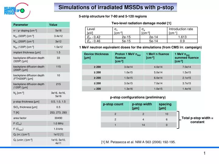
Simulations of irradiated MSSDs with p-stop. 5-strip structure for 7-80 and 5-120 regions. Two-level radiation damage model [1]. 1 MeV neutron equivalent doses for the simulations (from CMS irr. campaign). p-stop configurations (preliminary). Total p-stop width = constant.

E N D
Simulations of irradiated MSSDs with p-stop 5-strip structure for 7-80 and 5-120 regions Two-level radiation damage model [1] 1 MeV neutron equivalent doses for the simulations (from CMS irr. campaign) p-stop configurations (preliminary) Total p-stop width = constant [1] M. Petasecca et al. NIM A 563 (2006) 192-195.
Interstripcapacitances of measured and simulated non-irradiated 200P detectors @ +20 °C • Simulation dp= 1.5 μm • Qf= 5e10 cm-2 • Simulation dp= 1.5 μm • Qf= 5e10 cm-2 • region 5 • region 7 • Initial dip not produced by simulation • TEST ID: 15016 • TEST ID: 15010 • By lowering the value of Qffrom 5e10 cm-2to 2.7e10 cm-2the initial dip of measured curve is produced by simulation. At higher voltages simulated curve is within ~2 % of measurement. • At higher value of non-irradiated inversion layer oxide chargeQf= 4e11 cm-2 simulation does not match the measurement and fails at ~600 V due to high E at p-stop edges. • For the irradiation simulations, p-stop depth was varied by dp= 1.0 and 1.5 μm • Irradiated inversion layer oxide charge Qf = 1e12 cm-2 • region 7 • Simulation dp= 1.5 μm • Qf= 2.7e10 cm-2 • TEST ID: 15016
Irradiated 200P 7-80 region for varyingNp and p-stop count/width @ -20 °C • p-stop thickness = 1.0 μm • Widest wphas the lowest CintandVd • where minimumCintis reached • for Np=3e16 • Radiation damage removes electrons • from the inversion layer→ isolation • reached at lower Vd? • Cint • Cback • f = 1.0 MHz • f = 1.0 kHz • Are the strips are short-circuited for Np = 3e16 • until Vd has removed electrons from the inversion • layer? • e-density between two strips and p-stops for • Φ= 7e14 cm-2 and wp= 2μm. Isolation fails for • smallerNp @ low Vd? • Qf = 1e12 cm-2
Irradiated 200P 7-80 region for varyingNp and p-stop count/width @ +20 °C • p-stop thickness = 1.0 μm • Cback • At higher T electrons removed • from inversion layer more quickly • → min.Cintreached at lower Vd • 350 V (-20 °C) → 290 V (+20 °C) • Cint • e-densitybetween two strips and p-stops for • Φ= 7e14 cm-2 and wp= 2μm
Irradiated 200P 7-80 region for varyingNp and • p-stop count/width @ -/+20 °C • p-stop thickness = 1.5 μm= implant thickness • e-density between two strips and • p-stops for Φ = 7e14 cm-2 and wp= 2μm • Cint@ -20 °C • n@ -20 °C • No step in leakage current • observed for both Np • Ileak@ -20 °C • Cint@ +20 °C • No high values of Cint observed • after ~30 V • n@ +20 °C • Ileak@ +20 °C • Low e-density even at • low voltage for both Np • Superior configuration to dp = 1.0 μm