Download
1 / 16
160 likes | 167 Views
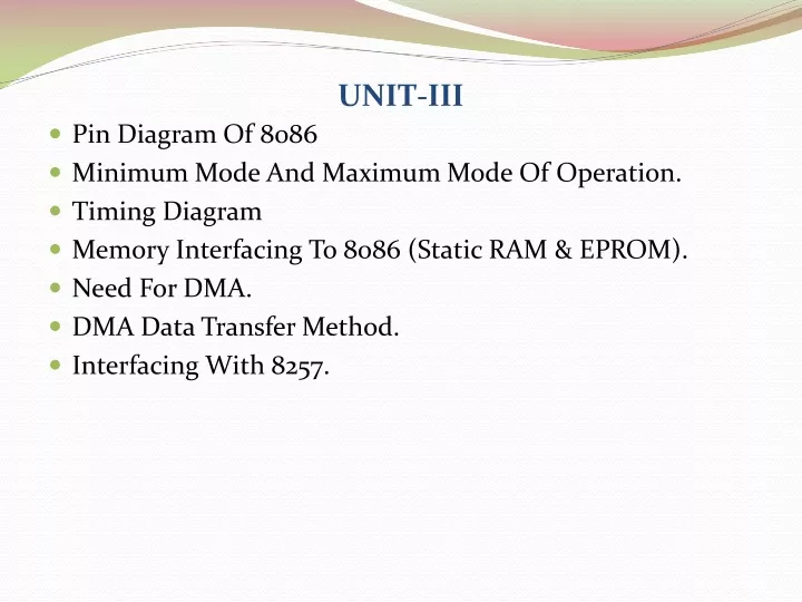
UNIT-III. Pin Diagram Of 8086 Minimum Mode And Maximum Mode Of Operation. Timing Diagram Memory Interfacing To 8086 (Static RAM & EPROM). Need For DMA. DMA Data Transfer Method. Interfacing With 8257. Fig 3.1 Pin diagram of 8086. Minimum mode of 8086.

E N D
UNIT-III • Pin Diagram Of 8086 • Minimum Mode And Maximum Mode Of Operation. • Timing Diagram • Memory Interfacing To 8086 (Static RAM & EPROM). • Need For DMA. • DMA Data Transfer Method. • Interfacing With 8257.
Minimum mode of 8086 • When the Minimum mode operation is selected, the 8086 provides all control signals needed to implement the memory and I/O interface. Fig 3.2 Minimum mode pin diagram of 8086
8086 in Maximum mode Fig 3.4 Maximum mode 8086 system
Memory interfacing Fig 3.6 Address mapping
DIRECT MEMORY ACCESS For the applications that require huge amounts of data transfer to memory from a magnetic or optical disk a dedicated hardware device called DMA controller is used. The DMA controller temporarily borrows the address bus ,data bus and control bus from the microprocessor and transfers the data bytes directly from the disk controller to a series of memory locations. Some DMA devices even can do memory to memory transfers.
Fig 3.12 Mode set register Bit format Fig 3.13 Statusregister Bit format