Download
1 / 39
390 likes | 393 Views
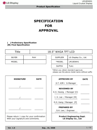
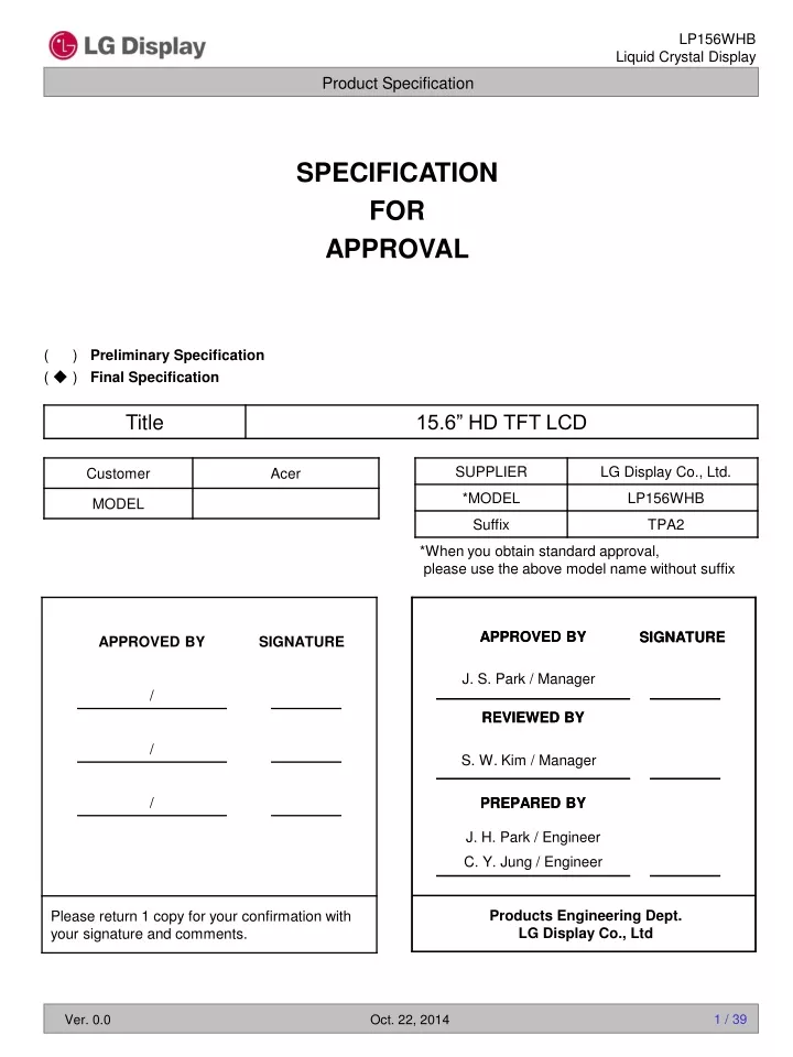
SPECIFICATION FOR APPROVAL. APPROVED BY. APPROVED BY. SIGNATURE. SIGNATURE. APPROVED BY. SIGNATURE. J. S. Park / Manager. /. REVIEWED BY. REVIEWED BY. /. S. W. Kim / Manager. PREPARED BY. PREPARED BY. /. J. H. Park / Engineer C. Y. Jung / Engineer. Products Engineering Dept.

E N D
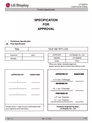
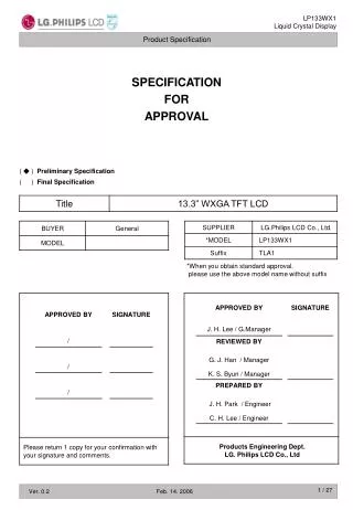
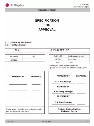
SPECIFICATION FOR APPROVAL APPROVED BY APPROVED BY SIGNATURE SIGNATURE APPROVED BY SIGNATURE J. S. Park / Manager / REVIEWED BY REVIEWED BY / S. W. Kim / Manager PREPARED BY PREPARED BY / J. H. Park / Engineer C. Y. Jung / Engineer Products Engineering Dept. LG Display Co., Ltd Please return 1 copy for your confirmation with your signature and comments.
1. General Description The LP156WHB is a Color Active Matrix Liquid Crystal Display with an integral LED backlight system. The matrix employs a-Si Thin Film Transistor as the active element. It is a transmissive type display operating in the normally white mode. This TFT-LCD has 15.6 inches diagonally measured active display area with HD resolution (1366 horizontal by 768 vertical pixel array). Each pixel is divided into Red, Green and Blue sub-pixels or dots which are arranged in vertical stripes. Gray scale or the brightness of the sub-pixel color is determined with a 6-bit gray scale signal for each dot, thus, presenting a palette of more than 262,144 colors. The LP156WHB has been designed to apply the interface method that enables low power, high speed, low EMI. The LP156WHB is intended to support applications where thin thickness, low power are critical factors and graphic displays are important. In combination with the vertical arrangement of the sub-pixels, the LP156WHB characteristics provide an excellent flat display for office automation products such as Notebook PC. EEPROM for EDID & T-Con TFT-LCD Panel (1366 x RGB x 768) User connector 30 Pin 1 1 1366 I2C Main Link Timing Controller Data Signal AUX HPD 768 Gate Signal DVCC Source Driver DVCC, AVDD ,Vcom, Gamma, Gate Signal Power Block VCC VLED VOUT_LED LED Backlight LED_EN LED Driver LED Cathode PWM General Features
90% 80% 60% 60 Wet Bulb Temperature [℃] 50 Humidity[(%)RH] Storage 40% 40 30 Operation 20 20% 10 0 10% -20 0 10 60 70 80 20 30 40 50 Dry Bulb Temperature [℃] 2. Absolute Maximum Ratings The following are maximum values which, if exceeded, may cause faulty operation or damage to the unit. Table 1. ABSOLUTE MAXIMUM RATINGS Note : 1. Temperature and relative humidity range are shown in the figure below. Wet bulb temperature should be 39C Max, and no condensation of water. Note : 2. Storage Condition is guaranteed under packing condition.
3. Electrical Specifications 3-1. LCD Electrical Characteristics Table 2. LCD ELECTRICAL CHARACTERISTICS Note) 1. The measuring position is the connector of LCM and the test conditions are under 25℃, fv = 60Hz 2. The specified ICC current and power consumption are under the VCC = 3.3V , 25℃, fv = 60Hz condition and Mosaic pattern. 3. The VCC rising time is same as the minimum of T1 at Power on sequence. 3.3V Rising time VCC 90% 10% 0V 0.5ms
3-2. LED Backlight Electrical Characteristics Table 3. LED B/L ELECTRICAL CHARACTERISTICS Note) 1. The measuring position is the connector of LCM and the test conditions are under 25℃. 2. The current and power consumption with LED Driver are under the VLED = 12.0V , 25℃, PWM Duty 100% and White pattern with the normal frame frequency operated(60Hz). 3. The VLED rising time is same as the minimum of T13 at Power on sequence. 4. The operation of LED Driver below minimum dimming ratio may cause flickering or reliability issue. 5. If Jitter of PWM is bigger than maximum, it may induce flickering. 6. This Spec. is not effective at 100% dimming ratio as an exception because it has DC level equivalent to 0Hz. In spite of acceptable range as defined, the PWM Frequency should be fixed and stable for more consistent brightness control at any specific level desired. 7. The life time is determined as the time at which brightness of LCD is 50% compare to that of minimum value specified in table 7. under general user condition. 12.0V Rising time VLED 90% 10% 0V 0.5ms
3-3. Interface Connections Table 4. MODULE CONNECTOR PIN CONFIGURATION (CN1)
3-3. eDP Signal Timing Specifications 3-3-1. Definition of Differential Voltage VD+ Common Mode Voltage VCM = (VD+ + VD-) / 2 VCM VDIFF VD- VCM VDIFF VDIFF = VD+ - VD- VDIFFp-p = (2* max | VD+ - VD-|) 0 V VDIFFp-p [ Definition of Differential Voltage ] 3-3-2. Main Link EYE Diagram 2 3 4 2 Volts Volts 1 5 1 3 8 7 6 4 0.0 0.1 0.2 0.3 0.4 0.5 0.6 0.7 0.8 0.9 1.0 0.0 0.1 0.2 0.3 0.4 0.5 0.6 0.7 0.8 0.9 1.0 UI UI [ EYE Mask at Source Connector Pins ] [ EYE Mask at Sink Connector Pins ] [ EYE Mask Vertices at Sink Connector Pins ] [ EYE Mask Vertices at Source Connector Pins ] [ EYE Mask Vertices at embedded DP Sink Connector Pins ]
3-3-3. eDP Main Link Signal ML_N Vbias Tx Vbias Rx 50Ω C_ML 50Ω 8 8 RX TX 50Ω 50Ω C_ML ML_P Source Connector Sink Connector [ Main Link Differential Pair ] Note) 1. Termination resistor is typically integrated into the transmitter and receiver implementations. 2. AC Coupling Capacitor isnot placed at the sink side. 3. In cabled embedded system, it is recommended the system designer ensure that EYE width and voltage are met at the sink side connector pins.
3-3-4. eDP AUX Channel Signal Aux_Ch_N Vbias Tx Vbias Rx 50Ω C_Aux 50Ω 8 8 AUX Ch. RX AUX Ch. RX AUX Ch. TX AUX Ch. TX 50Ω 50Ω C_Aux Aux_Ch_P Source Connector Sink Connector 8 8 [ Recommended eDP AUX Channel Differential Pair ] Note) 1. Termination resistor is typically integrated into the transmitter and receiver implementations. 2. AC Coupling Capacitor isnot placed at the sink side. 3. VAUX-DIFFp-p = 2*|VAUXP-VAUXN|
3-3-5. eDP HPD Signal HPD_TimeOut (2ms) HPD_IRQ Pulse (0.5 ~ 1.0ms) HPD Case1 : HPD IRQ Event Case3 : Hot Plug / Re-plug Event Case2 : Hot Unplug Event [ HPD Events ] Note) 1. HPD IRQ : Sink device wants to notify the Source device that Sink’s status has changed so it toggles HPD line, forcing the Source device to read its Link / Sink Receiver DPCD field via the AUX-CH 2. HPD Unplug : The Sink device is no longer attached to the Source device and the Source device may then disable its Main Link as a power saving mode 3. Plug / Re-plug : The Sink device is now attached to the Source device, forcing the Source device to read its Receiver capabilities and Link / Sink status Receiver DPCD fields via the AUX-CH
Data Enable, Hsync, Vsync tHP Hsync tCLK tWH 0.5 Vcc DCLK tHFP tWHA tHBP Condition : VCC =3.3V High: 0.7VCC Data Enable Low: 0.3VCC tVP tWV Vsync tVFP tWVA tVBP Data Enable 3-4. Signal Timing Specifications This is the signal timing required at the input of the User connector. All of the interface signal timing should be satisfied with the following specifications and specifications of eDP Tx/Rx for its proper operation. Table 4. TIMING TABLE Notice. all reliabilities are specified for timing specification based on refresh rate of 60Hz. However, LP156WHB has a good actual performance even at lower refresh rate (e.g. 40Hz or 50Hz) for power saving Mode, whereas LP156WHB is secured only for function under lower refresh rate. 60Hz at Normal mode, 50Hz, 40Hz at Power save mode. Don’t care Flicker level (Power save mode). 3-5. Signal Timing Waveforms
3-6. Color Input Data Reference The brightness of each primary color (red, green and blue) is based on the 6-bit gray scale data input for the color ; the higher the binary input, the brighter the color. The table below provides a reference for color versus data input. Table 5. COLOR DATA REFERENCE
3-7. Power Sequence T1 T11 90% Power Supply VCC T12 10% T2 T10 eDP Display Black Video Video From Source Black Video T3 HPD from Sink Sink Aux CH Aux Channel Operational T4 T7 Source Main Link Data Link Training Idle Valid Video Data Idle or off T5 T6 T8 T9 T13 T14 90% Power Supply VLED 10% T15 T16 Dimming signal Of LED B/L PWM PWM T17 T18 LED on/off Signal LED_EN Enabled Table 6. POWER SEQUENCE TABLE Note) 1. Do not insert the mating cable when system turn on. 2. Valid Data have to meet “3-3. eDP Signal Timing Specifications” 3. Video Signal, LED_EN and PWM need to be on pull-down condition on invalid status. 4. LGD recommend the rising sequence of VLED after the Vcc and valid status of Video Signal turn on.
4. Optical Specification Optical characteristics are determined after the unit has been ‘ON’ and stable for approximately 20 minutes in a dark environment at 25C. The values specified are at an approximate distance 50cm from the LCD surface at a viewing angle of and equal to 0. FIG. 1 presents additional information concerning the measurement equipment and method. FIG. 1 Optical Characteristic Measurement Equipment and Method LCD Module Equipment Optical Stage(x,y) 500mm±50mm Table 7. OPTICAL CHARACTERISTICS Ta=25C, VCC=3.3V, fV=60Hz
Note) 1. It should be measured in the center of screen(1 Point). Contrast Ratio(CR) is defined mathematically as Surface Luminance with all white pixels Contrast Ratio(1 Point) = Surface Luminance with all black pixels 2. Surface luminance is the average of 5 point across the LCD surface 50cm from the surface with all pixels displaying white. For more information see FIG 2. LWH = Average(1,2, … 5 Point) 3. The variation in surface luminance , The panel total variation ( WHITE) is determined by measuring N at each test position 1 through 13 and then defined as following numerical formula. For more information see FIG 2. Maximum (1,2, … 5 Point) Maximum (1,2, … 13 Point) WHITE (5P) = WHITE (13P) = Minimum (1,2, … 5 Point) Minimum (1,2, … 13 Point) 4. Response time is the time required for the display to transition from white to black (rise time, Tr) and from black to white (falling time, Tf). For additional information see FIG 3. 5. Viewing angle is the angle at which the contrast ratio is greater than 10. The angles are determined for the horizontal or x axis and the vertical or y axis with respect to the z axis which is normal to the LCD surface. For more information see FIG 4. 6. Gray scale specification
H A 10mm 10mm 6 7 8 3 2 B H,V : ACTIVE AREA V A : H/4 mm 9 10 1 B : V/4 mm POINTS: 13 POINTS 4 5 13 11 12 Active Area Tf Tr % 100 90 Optical Response 10 0 white white black FIG. 2 Luminance <Measuring point for Average Luminance & measuring point for Luminance variation> FIG. 3 Response Time The response time is defined as the following figure and shall be measured by switching the input signal for “black” and “white”. FIG. 4 Viewing angle <Dimension of viewing angle range>
5. Mechanical Characteristics The contents provide general mechanical characteristics for the model LP156WHB. In addition the figures in the next page are detailed mechanical drawing of the LCD.
<FRONT VIEW> Note) Unit:[mm], General tolerance: 0.5mm
<REAR VIEW> Note) Unit:[mm], General tolerance: 0.5mm
6. Reliability Environment test condition { Result Evaluation Criteria } There should be no change which might affect the practical display function when the display quality test is conducted under normal operating condition.
7. International Standards 7-1. Safety a) UL 60950-1, Underwriters Laboratories Inc. Information Technology Equipment - Safety - Part 1 : General Requirements. b) CAN/CSA-C22.2 No. 60950-1-07, Canadian Standards Association. Information Technology Equipment - Safety - Part 1 : General Requirements. c) EN 60950-1, European Committee for Electro technical Standardization (CENELEC). Information Technology Equipment - Safety - Part 1 : General Requirements. d) IEC 60950-1,The International Electro technical Commission (IEC). Information Technology Equipment - Safety - Part 1 : General Requirements 7-2. Environment a) RoHS, Directive 2011/65/EU of the European Parliament and of the council of 8 June 2011
Year 2011 2012 2013 2014 2015 2016 2017 2018 2019 2020 Mark A B C D E F G H J K Month Jan Feb Mar Apr May Jun Jul Aug Sep Oct Nov Dec Mark 1 2 3 4 5 6 7 8 9 A B C 8. Packing 8-1. Designation of Lot Mark a) Lot Mark A B C D E F G H I J K L M A,B,C : SIZE(INCH) D : YEAR E : MONTH F ~ M : SERIAL NO. N O P Q (Not included in barcode) N: PANEL FACTORY O : MODULE FACTORY P ~ Q: SERIAL NO. Note 1. YEAR 2. MONTH 3. Factory Code b) Location of Lot Mark Serial No. is printed on the label. The label is attached to the backside of the LCD module. This is subject to change without prior notice. ※ For your better understanding, please see the label on the drawing in page 21 8-2. Packing Form a) Package quantity in one box : 20pcs b) Box Size : 478mm X 365mm X 328mm
9. PRECAUTIONS Please pay attention to the followings when you use this TFT LCD module. 9-1. MOUNTING PRECAUTIONS (1) You must mount a module using holes arranged in four corners or four sides. (2) You should consider the mounting structure so that uneven force (ex. Twisted stress) is not applied to the module. And the case on which a module is mounted should have sufficient strength so that external force is not transmitted directly to the module. (3) Please attach the surface transparent protective plate to the surface in order to protect the polarizer. Transparent protective plate should have sufficient strength in order to the resist external force. (4) You should adopt radiation structure to satisfy the temperature specification. (5) Acetic acid type and chlorine type materials for the cover case are not desirable because the former generates corrosive gas of attacking the polarizer at high temperature and the latter causes circuit break by electro-chemical reaction. (6) Do not touch, push or rub the exposed polarizers with glass, tweezers or anything harder than HB pencil lead. And please do not rub with dust clothes with chemical treatment. Do not touch the surface of polarizer for bare hand or greasy cloth.(Some cosmetics are detrimental to the polarizer.) (7) When the surface becomes dusty, please wipe gently with absorbent cotton or other soft materials like chamois soaks with petroleum benzene. Normal-hexane is recommended for cleaning the adhesives used to attach front / rear polarizers. Do not use acetone, toluene and alcohol because they cause chemical damage to the polarizer. (8) Wipe off saliva or water drops as soon as possible. Their long time contact with polarizer causes deformations and color fading. (9) Do not open the case because inside circuits do not have sufficient strength. (10) When handling the LCD module, it needs to handle with care not to give mechanical stress to the PCB and Mounting Hole area.” 9-2. OPERATING PRECAUTIONS (1) The spike noise causes the mis-operation of circuits. It should be lower than following voltage : V=± 200mV(Over and under shoot voltage) (2) Response time depends on the temperature.(In lower temperature, it becomes longer.) (3) Brightness depends on the temperature. (In lower temperature, it becomes lower.) And in lower temperature, response time(required time that brightness is stable after turned on) becomes longer. (4) Be careful for condensation at sudden temperature change. Condensation makes damage to polarizer or electrical contacted parts. And after fading condensation, smear or spot will occur. (5) When fixed patterns are displayed for a long time, remnant image is likely to occur. (6) Module has high frequency circuits. Sufficient suppression to the electromagnetic interference shall be done by system manufacturers. Grounding and shielding methods may be important to minimized the interference.
9-3. ELECTROSTATIC DISCHARGE CONTROL Since a module is composed of electronic circuits, it is not strong to electrostatic discharge. Make certain that treatment persons are connected to ground through wrist band etc. And don’t touch interface pin directly. 9-4. PRECAUTIONS FOR STRONG LIGHT EXPOSURE Strong light exposure causes degradation of polarizer and color filter. 9-5. STORAGE When storing modules as spares for a long time, the following precautions are necessary. (1) Store them in a dark place. Do not expose the module to sunlight or fluorescent light. Keep the temperature between 5C and 35C at normal humidity. (2) The polarizer surface should not come in contact with any other object. It is recommended that they be stored in the container in which they were shipped. 9-6. HANDLING PRECAUTIONS FOR PROTECTION FILM (1) When the protection film is peeled off, static electricity is generated between the film and polarizer. This should be peeled off slowly and carefully by people who are electrically grounded and with well ion-blown equipment or in such a condition, etc. (2) The protection film is attached to the polarizer with a small amount of glue. If some stress is applied to rub the protection film against the polarizer during the time you peel off the film, the glue is apt to remain on the polarizer. Please carefully peel off the protection film without rubbing it against the polarizer. (3) When the module with protection film attached is stored for a long time, sometimes there remains a very small amount of glue still on the polarizer after the protection film is peeled off. (4) You can remove the glue easily. When the glue remains on the polarizer surface or its vestige is recognized, please wipe them off with absorbent cotton waste or other soft material like chamois soaked with normal-hexane. 9-7. THE LGD QA RESPONSIBILITY WILL BE AVOIDED IN CASE OF BELOW • When the customer attaches TSM(Touch Sensor Module) on LCM without Supplier’s approval. • When the customer attaches cover glass on LCM without Supplier’s approval. • (3) When the LCMs were repaired by 3rd party without Supplier’s approval. • (4) When the LCMs were treated like Disassemble and Rework by the Customer and/or Customer’s • representatives without supplier’s approval.
APPENDIX A. LGD Proposal for system cover design b a LCM PAD Back cover Boss ◆ a : min 0mm ◆ b : min 0.3mm, Max 1.0mm Boss PAD Back cover T-CON T-CON OK NG
APPENDIX A. LGD Proposal for system cover design Wire OK NG flange push LCM boss boss PAD boss Pad boss boss Back cover Back cover Pad Back cover Back cover Boss push crack OK NG
APPENDIX A. LGD Proposal for system cover design LCM LCM Back cover Back cover Rib Bracket OK OK LCM LCM Back cover Back cover NG CO a Front cover LCM Back cover [OK]a ≥ 0.3mm [CO] 0.3mm ≥ a ≥ 0.1mm [NG] a ≤ 0.1mm
APPENDIX A. LGD Proposal for system cover design Light leakage Front cover Front cover LCM LCM Back cover Back cover OK NG Back cover OK Back cover NG
APPENDIX A. LGD Proposal for system cover design a [OK]a ≤ 0.3mm [CO] 0.5mm ≥ a ≥ 0.3mm [NG] a ≥ 0.5mm Mouse pad OK NG Keyboard Keyboard push push crack OK NG
APPENDIX A. LGD Proposal for system cover design Panel BLU Back cover FPC A a A’ Rib, Frame … Externalshock a ≥ 0.5mm [at max dimension of design] a ≥ 1.0mm [at typical dimension of design] OK NG a crack LCM a ≥ 0.5mm [at max dimension of design] a ≥ 1.0mm [at typical dimension of design] Rib Back cover
APPENDIX B. LGD Proposal for eDP Interface Design Guide LCDVCC LCDVCC 0~200ms 0~200ms HPD Glitch HPD Glitch Min 2.0V Min 2.0V HPD HPD Hot Plug Event No AUX communication Hot Plug Event AUX communication AUX AUX Abnormal AUX communication by system HPD glitch recognition Normal AUX communication by system HPD recognition [ Abnormal Communication By HPD Glitch ] [ Normal Communication By HPD Signal ] LCDVCC HPD_IRQ by link disconnecting 0.5ms ~ 1.0ms RX link status check & Re-link training HPD Abnormal Status Link disconnect Ex) HPD Pulse AUX Link training Link training Normal Video stream Normal Video stream Main link
APPENDIX B. LGD Proposal for eDP Interface Design Guide [EYE Diagram] 350mV 2 3 4 150mV 2 214.8ps Volts 188.5ps 1 5 Volts 1 3 8 7 6 0.0 0.1 0.2 0.3 0.4 0.5 0.6 0.7 0.8 0.9 1.0 4 UI 0.0 0.1 0.2 0.3 0.4 0.5 0.6 0.7 0.8 0.9 1.0 UI [EYE Vertices for TP3 at HBR] [EYE Vertices for TP2 at HBR]
APPENDIX B. LGD Proposal for eDP Interface Design Guide * LGD recommend that Source must power off the LCDVCC if Main Link off like below. Vcc Vcc Main Link Main Link [Case1. Resolution Change] [Case2. Close the Lid]
APPENDIX B. LGD Proposal for eDP Interface Design Guide Abnormal Main Link Signal Normal Main Link Signal PSR Wake up from AUX PSR Wake up from AUX [ Abnormal Main Link Noise ] [ Normal Main Link Signal ]
APPENDIX C. Enhanced Extended Display Identification Data (EEDIDTM) 1/3
APPENDIX C. Enhanced Extended Display Identification Data (EEDIDTM) 2/3
APPENDIX C. Enhanced Extended Display Identification Data (EEDIDTM) 3/3