Download
1 / 19
200 likes | 348 Views
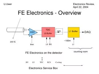
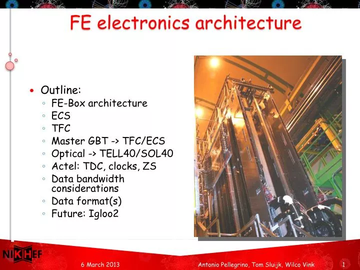
FE electronics architecture. Outline: FE-Box architecture ECS TFC Master GBT -> TFC/ECS Optical -> TELL40/SOL40 Actel : TDC, clocks, ZS Data bandwidth considerations Data format(s) Future: Igloo2. Upgrade old -> new. GOL board -> Master GBT board OTIS board -> TDC Board

E N D
FE electronics architecture • Outline: • FE-Box architecture • ECS • TFC • Master GBT -> TFC/ECS • Optical -> TELL40/SOL40 • Actel: TDC, clocks, ZS • Data bandwidth considerations • Data format(s) • Future: Igloo2 Antonio Pellegrino, Tom Sluijk, Wilco Vink
Upgrade old -> new • GOL board -> Master GBT board • OTIS board -> TDC Board • Control Box -> none • ASDBLR -> unchanged GBT Master board TDC Board left TDC Board right Antonio Pellegrino, Tom Sluijk, Wilco Vink
OT Front-end boxes • 432 Front end boxes, each: • 1 master GBT / power board (replaces: GOL board) • 1 Master GBT • TFC distribution • 1 SCA • Optical RxTx • CERN SM01C DC/DC conv. • 4 TDC boards (replaces: OTIS boards) • Actel Proasic3E • 2 data GBT’s • 1 SCA • 8 ASDBLR boards • Total: • 3888 GBT’s • 432 TFC Master GBT’s (Bidir) • 3456 Data GBT’s • 2160 SCA’s Tom Sluijk, Wilco Vink, Antonio Pellegrino
Front end Box ECS • GBT master board • 1 SCA • Power • Temperature • Optical devices • 4 Actel TDC boards each • 1 SCA • Actel re-programming via JTAG • GBT configuration • 4 Threshold DAC • Temperature monitoring • Soft reset Actel • I2C -> FPGA registers Antonio Pellegrino, Tom Sluijk, Wilco Vink
Front end box TFC • Master GBT Clkout to 8 GBT’s • GBT’s as Fan-out • Programmable delay/phase • Clock for Actel from “data” GBT: • BxClk • TestPulseClk • TFC Clk • TDC Clocks(fall-back) • TFC distribution • BxRst, FeRst, Sync, NZS, HdrOnly, BxVeto, CalibType(3:0), SnapShot Antonio Pellegrino, Tom Sluijk, Wilco Vink
Master GBT (FE) <-> TFC/ECS • 4+1 SCA e-links • 8 bits • 2 bits(1 e-link Master GBT-SCA) • We need TFC Fan-out: • 4 TDC boards, each: • BxRst, FeRst, Sync, NZS, HdrOnly, BxVeto, CalibType(3:0), SnapSh • 4*11 bits • SLVS -> LVDS buffer -> TFC fan-out • OR: • GBT As TFC fan-out • Use unused SCA and empty as duplicate TFC signals • Total: 52 bits / 25ns (of 80) • Dedicated TFC word for OT ? • All outputs on 40 MHz, SCA on 40 MHz ?? From LHCb-INT-2012-018 Antonio Pellegrino, Tom Sluijk, Wilco Vink
GBT gigabit <-> optical • Master GBT • Versatile link bi-directional VRTx • Data GBT: 8 (or 4) links • Optical link details in talk Tom • KK Ghan Option: • 12 way Vcsel driver • Eight links Four Spares • 1 MPO connector / FE-Box • 4 (or 2) VTTx • Versatile link option Antonio Pellegrino, Tom Sluijk, Wilco Vink
Actel TDC • 4, 8-bit shift registers • 32 bits hitregister • 5 Bits TDC + Valid bit • Complex timing • PLL 320 MHz output Duty Cycle != 50% • 32 Hit inputs Antonio Pellegrino, Tom Sluijk, Wilco Vink
Actel TDC • ActelProAsic A3PE1500FG484 (4 FPGA’s/FE-box) • 32 channel 5 bits TDC • Based on 4 320 MHz clocks(2 edges and 90phase shifted) • fixed placement (3 variants: top, right, bottom) • Hit inputs located at fixed length from pins • Zero suppression • Two wide-bus 28bits@160MHz GBT outputs Antonio Pellegrino, Tom Sluijk, WilcoVink,
Actel Clocking scheme • Actel clock usage • 3(6) Pll’s: 1*TDC, 2* GBT • Chip globals: Tot:6 • 40(BxClk),80,320, 320ph90 • Resets: Soft I2C rst, Hard Reset • Quadrant globals: Tot:4*3 • GBT1 bus: 80,160 • GBT2 bus: 80,160 Antonio Pellegrino, Tom Sluijk, Wilco Vink
Zero Suppression • 16/32 Channel suppress mechanism • (4 channel example) • Valid channels are staggered from LSB • 16/32 channels needs 16/32 clock cycles • Active channel/position in fixed relation with hitpattern Antonio Pellegrino, Tom Sluijk, Wilco Vink
FPGA Resource usage CORE Used: 14776 Total: 38400 (38.48%) IO (W/ clocks) Used: 236 Total: 280 (84.29%) Differential IO Used: 102 Total: 139 (73.38%) GLOBAL (Chip+Quadrant) Used: 12 Total: 18 (66.67%) PLL Used: 3 Total: 6 (50.00%) RAM/FIFO Used: 22 Total: 60 (36.67%) Low Static ICC Used: 0 Total: 1 (0.00%) FlashROM Used: 0 Total: 1 (0.00%) User JTAG Used: 0 Total: 1 (0.00%) Antonio Pellegrino, Tom Sluijk, Wilco Vink
Bandwidth considerations: • One Design two options • Design for “100% occupancy” • One GBT per 16 channels • 8 data GBT’s per Front-end Box • Max data rate NZS, 100% lumi • 80b TDC + 16b hitpattern + 8b Status + 4b Bcid /25ns • Design for cost optimization • One GBT per 32 channels • 4 GBT’s per front end • Max occupancy37% • 160b TDC + 32b hitpattern + 8b Status + 4b Bcid /25ns • Half TELL40’s , optical links, GBT’s • ……. • Talk from Tom(#links etc) Antonio Pellegrino, Tom Sluijk, Wilco Vink
Two 16 ch. TDC in one FPGA Dual GBT’s Hit 16 channel TDC Zero-supp 16 stages Fifo Readout GBT1 3*PLL Control / Monitoring TFC/ECS Hit 16 channel TDC Zero-supp 16 stages Fifo Readout GBT2 Actel FPGA GBT1 27 0 16 bits Hit pattern channel (0-15) 4 bits BX cnt 8 bits Status Padded ‘0’ 5 bits Data 5 bits Data 5 bits Data 5 bits Data 5 bits Data Max 4 words when all channels are hit GBT2 16 bits Hit pattern channel (16-31) 4 bits BX cnt 8 bits Status Padded ‘0’ 5 bits Data 5 bits Data 5 bits Data 5 bits Data Max 4 words when all channels are hit Data Format (9 channels hit): Antonio Pellegrino, Tom Sluijk, WilcoVink,
NZS data Antonio Pellegrino, Tom Sluijk, Wilco Vink
32 channel TDC with single GBT 32 channel TDC Zero-supp 32 stages Fifo Readout GBT 3*PLL Control / Monitoring TFC/ECS Actel FPGA Data Format (9 channels hit): GBT 27 0 16 bits Hit pattern channel (0-15) 4 bits BX cnt 8 bits Status Data 5 bits Data 5 bits Data 16 bits Hit pattern channel(16-31) 5 bits Data 5 bits Data 5 bits Data 5 bits Data 5 bits Data 5 bits Padded ‘0’ s 5 bits Dat Max 8 words when all channels are hit Antonio Pellegrino, Tom Sluijk, WilcoVink,
Example ZS data stream E.g. Antonio Pellegrino, Tom Sluijk, Wilco Vink
Igloo2 Some thoughts…. • ACTEL MICROSEMI announces this summer Igloo2 • Igloo2 • (SEU immune) Flash based • 65nm technology • 5Gbs SerDes • SEU tolerant memories • Upto 100kRad ?? • Needs Radiation tests. • Student project planned after summer holiday, with Smartfusion2 (@Nikhef) • Waiting for delivery Dev. Board. • Implement/transfer TDC design Proasic3E -> Igloo2 • Smartfusion2: ARM + FPGA(=Igloo2) • Microsemi document: Design for Igloo2 with Smartfusion2 • To be used in ….??? Antonio Pellegrino, Tom Sluijk, WilcoVink
Plans • 4*432 + spares TDC boards • 1*432 + spares GBT master boards • To be produced and tested before 2018 • See Tom’s talk about installation • In between: • Proto types • Test and characterize • … Antonio Pellegrino, Tom Sluijk, Wilco Vink