Download

1 / 39
390 likes | 490 Views
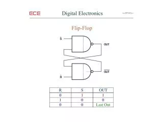
EE24C Digital Electronics Projects. Counters and Registers. Definitions. A synchronous circuit is a sequential circuit whose input/output changes are synchronized by a reference signal called clock signal. Basic synchronous circuits include:

E N D
EE24C Digital Electronics Projects Counters and Registers
Definitions • A synchronous circuit is a sequential circuit whose input/output changes are synchronized by a reference signal called clock signal. • Basic synchronous circuits include: • Counters (sequential circuits configure in a specific form in order to count clock ticks). • Registers (for elementary storage and shift operations) • Random-Access Memories (RAMs) for Read/write operations.
Basic Synchronous Circuits • Characteristics: • Clocked by stable clock signal (crystal oscillator) • Set of input and output data lines • Set of control signals • Can be described using FSMs • Can be implemented using basic synchronous cells (DFFs and JKFFs). • Exist as MSI (medium scale integrated) circuits. • Their designs often require the use of some combinational elements.
Parallel Load Register • Characteristics: • A n-bit parallel load register is an ordered set of n FFs that are used to store n-bit word. • It has n-bit input and n-bit Output Data • A set of control signals: Load (LD), Clear (CLR)
Inputs: X = (xn-1, xn-2,…x0), xi{0,1} LD, CLR {0,1} Outputs: Z = (zn-1,…, z0) zi{0,1} State: S = (Sn-1, …, S0), Si{0,1} Figure: N-bit parallel register. Function: State Transition and Output functions
How can we design a n-bit register from the specification given previously? • By analyzing the specification, it appears that DFFs can be used in order to implement the Load operation. • The outputs of the register change according to the values of the two control signals LD and CLR Use of a MUX • We must avoid the condition LD = CLR=1.
4-Bit parallel Register: Parallel load registers exist in different MSI flavors.
Multibit registers and latches • 74x175
8-bit (octal) register • 74x374 • 3-state output Active on a high level.
Other octal registers • 74x273 • asynchronous clear • 74x377 • clock enable
Octal latch • 74x373 • Output enable • Latch-enable input “C” or “G” • Register vs. latch, what’s the difference? • Register: edge-triggered behavior • Latch: output follows input when G is asserted
Shift Registers • There are many situations in digital systems design where it’s useful to be able to shift the contents of a register to the left or the right. • A right-shift operation changes the register states as follows: • (0, zn-1, zn-2, ……..z1) (zn-1, zn-2, ………..z1, z0), • A left shift performs the transformation: • (zn-2, ………..z1, z0,0) (zn-1, zn-2, ………..z1, z0)
A shift register is an n-bit register with a provision for shifting its stored data by one bit position at each clock ticks. • We have different configurations: • Serial-in/Serial-out shift register • Serial-in/Parallel-out shift register (for serial-to-parallel conversion) • Parallel-in/Serial-out shift register (for parallel-to-serial conversion)
A register organized to allow left- or right-shift operations of this kind is called a shift register. The following shows a block diagram of a universal registers with load and shift features.
The high-level specification of the universal register is given as follows
The following figure shows a 4-bit bidirectional shift register
Serial-to-parallel conversion • Use a serial-in, parallel-out shift register
mux Parallel-to-serial conversion • Use parallel-in, serial-out shift register
Do both • Parallel-in, parallel-out shift register
“Universal” shift register74x194 • Shift left • Shift right • Load • Hold
Counters • A counter is a simple sequential machine designed to cycle through a predetermined sequence of p distinct states S0, S1,…..Sp-1 in response to pulses on an input line. The p states usually represent k consecutive numbers; the state transitions can be thus described by the expression Si+1 Si + 1 (modulo k). (Si = s(t) and Si+1 = s(t+1) • Each input pulse increments the state by 1; the machine can therefore be viewed as counting the input pulses. • Counters come in many different varieties depending on the number codes used, the modulus p, and the timing mode (synchronous or asynchronous)
Type of counter (up or down): The simplest counters can be obtained by minor modifications of an ordinary register or a shift register. The next figure shows a modulo-16 binary counter composed of four JK flip-flops. This circuit counts the pulses on the count enable line. Note that the output of each flip-flop may alter the state of its right neighbour, so that the "carry" signal ripple through the counter from left to right. This type of counter is therefore called ripple counter (asynchronous) counter.
Figure: A modulo-16 ripple counter: (a) logic diagram; (b) symbol.
A counter is basically a serial-input parallel-output device. As in the case of shift registers, it can be useful to have a parallel load capability. Another refinement that is occasionally useful is to permit the counter to be decremented as well as incremented (Up-Down counter). Counters are also available whose modulus can be altered by means of modulus-select control lines; such counters are frequently termed programmable.
The specification of a binary counter with parallel in puts is given as follows:
An illustration of a modulo-16 binary counter of this type is given in the figure below. A modulo-16 binary counter with parallel input.
74x163 MSI 4-bit counter A parallel-load up/down counter
Counter operation • Free-running 16 • Count if ENP andENT both asserted. • Load if LD is asserted(overrides counting). • Clear if CLR is asserted (overrides loading and counting). • All operations take place on rising CLK edge. • RCO is asserted if ENT is asserted andCount = 15.
Free-running 4-bit ’163 counter • “divide-by-16” counter
Modified counting sequence • Load 0101 (5) after Count = 15 • 5, 6, 7, 8, 9, 10, 11, 12, 13, 14, 15, 5, 6, … • “divide-by-11” counter
trick to save gate inputs Another way • Clear after Count = 1010 (10) • 0, 1, 2, 3, 4, 5, 6, 7, 8, 9, 10, 0, 1, 2, 3, … • “modulo-11” or “divide-by-11” counter
Cascading counters • RCO (ripple carry out) is asserted in state 15, if ENT is asserted.