Download
1 / 51
600 likes | 946 Views
THE LIGHT EMITTING DIODE. Chapter 6. When the electron falls down from conduction band and fills in a hole in valence band, there is an obvious loss of energy. CB. VB. The question is; where does that energy go?.

E N D
THE LIGHT EMITTING DIODE Chapter 6
When the electron falls down from conduction band and fills in a hole in valence band, there is an obvious loss of energy. CB VB The question is; where does that energy go?
In order to achieve a reasonable efficiency for photon emission, the semiconductor must have a direct band gap. CB VB The question is; what is the mechanism behind photon emission in LEDs?
E For example; Silicon is known as an indirect band-gap material. What this means is that as an electron goes from the bottom of the conduction band to the top of the valence band; it must also undergo a significant change in momentum. CB k VB
As we all know, whenever something changes state, one must conserve not only energy, but also momentum. • In the case of an electron going from conduction band to the valence band in silicon, both of these things can only be conserved: The transition also creates a quantized set of lattice vibrations, called phonons, or "heat“ .
Phonons possess both energy and momentum. • Their creation upon the recombination of an electron and hole allows for complete conservation of both energy and momentum. • All of the energy which the electron gives up in going from the conduction band to the valence band (1.1 eV) ends up in phonons, which is another way of saying that the electron heats up the crystal.
In a class of materials called direct band-gap semiconductors; • the transition from conduction band to valence band involves essentially no change in momentum. • Photons, it turns out, possess a fair amount of energy ( several eV/photon in some cases ) but they have very little momentum associated with them.
Thus, for a direct band gap material, the excess energy of the electron-hole recombination can either be taken away as heat, or more likely, as a photon of light. • This radiative transition then conserves energy and momentum by giving off light whenever an electron and hole recombine. CB This gives rise to (for us) a new type of device; the light emitting diode (LED). VB
e- e- Mechanism behind photon emission in LEDs? Mechanism is “injection Electroluminescence”. Luminescence part tells us that we are producing photons. Electro part tells us that the photons are being produced by an electric current. Injection tells us that photon production is by the injection of current carriers.
Producing photon Electrons recombine with holes. e- h CB Energy of photon is the energy of band gap. VB
Method of injection • We need putting a lot of e-’s where there are lots of holes. • So electron-hole recombination can occur. • Forward biasing a p-n junction will inject lots of e-’s from n-side, across the depletion region into the p-side where they will be combine with the high density of majority carriers. I - + n-side p-side
Notice that: • Photon emission occurs whenever we have injected minority carriers recombining with the majority carriers. • If the e- diffusion length is greater than the hole diffusion length, the photon emitting region will be bigger on the p-side of the junction than that of the n-side. • Constructing a real LED may be best to consider a n++p structure. • It is usual to find the photon emitting volume occurs mostly on one side of the junction region. • This applies to LASER devices as well as LEDs.
MATERIALS FOR LEDS • The semiconductor bandgap energy defines the energy of the emitted photons in a LED. • To fabricate LEDs that can emit photons from the infrared to the ultraviolet parts of the e.m. spectrum, then we must consider several different material systems. • No single system can span this energy band at present, although the 3-5 nitrides come close. CB VB
Unfortunately, many of potentialllyuseful 2-6 group of directband-gapsemiconductors (ZnSe,ZnTe,etc.) comenaturallydopedeither p-type, or n-type, but theydon’tliketo be type-convertedbyoverdoping. • Thematerialreasonsbehindthisarecomplicatedand not entirelywell-known. • Thesame problem is encountered in the 3-5 nitridesandtheiralloysInN, GaN, AlN, InGaN, AlGaN, andInAlGaN. Theamazingthingabout3-5 nitridealloysystems is thatappearto be directgapthroughout.
Whenwe talk aboutlight ,it is conventionaltospecifyitswavelength, λ, instead of itsfrequency. • Visiblelight has a wavelength on theorder of nanometers. • Thus, a semiconductor with a 2 eV band-gap should give alight at about 620 nm (in thered). A 3 eV band-gap material would emit at 414 nm, in the violet. • The human eye, ofcourse, is not equally responsive to all colors.
Relative response of the human eye to various colors Relative eye response 100 10-1 10-2 10-3 10-4 GaAs.14p86 GaAs.35p65 GaAs.6p4 GaP:N GaN ZnSe violet blue green yellow orange red 350 400 450 500 550 600 650 700 750 Wavelength in nanometers The materials which are used for important light emitting diodes (LEDs) for each of the different spectral regions.
Properties of InGaN • InGaNalloy has onecomposition at a time only. • Thismaterialwillemitonewavelengthonlycorrespondingtothisparticularcomposition. • An InGaN LED wouldnot emitwhitelight(thewhole of thevisiblespectrum at once) since itsspecificcomposition. • For a whitelightsourcewehaveto form a complicatedmultilayer device emittinglots of differentwavelengths.
Properties of InGaN • A LED fabricatedin a gradedmaterialwhere on eitherside of thejunctionregionthematerialchangesslowlyfromInNtoGaNviaInGaNalloys. • Minoritycarriersneedtogetthroughthewhole of thisalloyregionifefficientphotonproduction at allvisiblewavelengthswastooccur.
GaN InN ultraviolet 3.3 eV(376 nm)
GaN InN violet 3 eV (414 nm)
GaN InN 2.7 eV(460 nm)
GaN InN 2.4 eV(517 nm)
GaN InN 2.1 eV(591 nm)
GaN InN 2 eV(620 nm) 2.00 eV
A number of the important LEDs are based on the GaAsP system. GaAs is a direct band-gap S/C with a band gap of 1.42 eV (in the infrared). GaP is an indirect band-gap material with a band gap of 2.26 eV (550nm, or green). GaAs GaP 1.42 eV
GaAs GaP 1.52 eV
GaAs GaP 1.62 eV
GaAs GaP 1.72 eV
GaAs GaP 1.80 eV
GaAs GaP 1.90 eV
GaAs GaP 2.00 eV
GaAs GaP 2.26 eV
Addition of a nitrogenrecombinationcentertoindirectGaAsP . • Both As and P aregroup V elements. (Hencethenomenclature of thematerials as III-V compoundsemiconductors.) _ Energy + Momentum
We can replacesome of theAs with P in GaAsandmake a mixedcompoundsemiconductorGaAs1-xPx. • Whenthemolefraction of phosphorous is lessthanabout 0.45 thebandgap is direct, andsowe can "engineer" thedesiredcolor of LED thatwewantbysimplygrowing a crystalwiththeproperphosphorusconcentration!
(a) Direct-gap GaAs (b) Crossover GaAs0.50P0.50 (c) Indirect-gap GaP X CB Minimum N Level Γ CB Minimum N Level N Level Γ VB Maximum Schematic band structure of GaAs, GaAsP, and GaP. Also shown is the nitrogen level. At a P mole fraction of about 45-50 %, the direct-indirect crossover occurs.
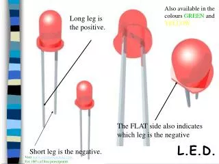
Materials for visible wavelength LEDs • We see them almost everyday, either on calculator displays or indicator panels. • Red LED use as “ power on” indicator • Yellow, green and amber LEDs are also widely available but very few of you will have seen a blue LED.
N-GaAsP P = 40 % p-GaAsP region N-GaAs substrate Ohmic Contacts Dielectric (oxide or nitride) Fig. GaAsP RED LED on a GaAs sub. Red LEDs • can be made in the GaAsP (gallium arsenide phosphide). • GaAs1-xPx • for 0<x<0.45 has direct-gap • for x>0.45 the gap goes indirect and • for x=0.45 the band gap energy is 1.98 eV. • Hence it is useful for red LEDs.
Isoelectronic Centre • Isoelectronicmeansthat the centre being introduced has the same number of valance electrons as the element it is replacing. • For example, nitrogen can replace some of the phosphorus in GaP. It is isoelectronic with phosphorus, but behaves quite differently allowing reasonably efficient green emission.
E CB edge electrons Isoelectronic centre dE Electron-hole recombination Holes VB edge k = 0 How isoelectronic centres work? • For our isoelectronic centre the position is very well-defined, hence there is a considerable spread in its momentum state. • Isoelectronic centre has the same valance configuration as the phosphorus it is replacing. • It doesn't act as a dopant.
E CB edge electrons Isoelectronic centre dE Electron-hole recombination Holes VB edge k = 0 Isoelectronic centres provide a ‘stepping stone’ for electrons in E-k space so that transitions can occur that are radiatively efficient. The recombination event shown has no change in momentum, so it behaves like a direct transition. Because the effective transition is occurring between the isoelectronic centre and VB edge, the photon that is emitted has a lower energy than the band-gap energy.
E CB edge electrons Isoelectronic centre dE Electron-hole recombination Holes VB edge k = 0 GaP : N • (dE = 50 meV) Photon energy is less than the semiconductor band-gap energy it means that the photon is not absorbed by the semiconductor, and so the photon is easily emitted from the material. • This lack of absorption pushes up the efficiency of the diode as a photon source. 50 meV
For emission in the red part of the spectrum using GaP the isoelectronic centre introduced contains zinc (Zn) and oxygen (O). These red LEDs are usually designated GaP:ZnO and they are quite efficient. • Their main drawback is that their emission at 690 nm is in a region where the eye sensitivity is rather low, which means that commercially, the AlGaAs/GaAs diodes are more successful devices.
Orange-Yellow & Green LEDs • Orange (620 nm) and yellow (590 nm) LEDs are commercially made using the GaAsP system. However, as we have just seen above, the required band-gap energy for emission at these wavelengths means the GaAsP system will have an indirect gap. • The isoelectronic centre used in this instance is nitrogen, and the different wavelengths are achieved in these diodes by altering the phosphorus concentration. • The green LEDs (560 nm) are manufactured using the GaP system with nitrogen as the isoelectronic centre.
Blue LEDs • Blue LEDs are commercially available and are fabricated using silicon carbide (SiC). Devices are also made based on gallium nitride (GaN). • Unfortunately both of these materials systems have major drawbacks which render these devices inefficient. • The reason silicon carbide has a low efficiency as an LED material is that it has an indirect gap, and no ‘magic’ isoelectronic centre has been found to date.
Blue LEDs The transitions that give rise to blue photon emission in SiC are between the bands and doping centres in the SiC. The dopants used in manufacturing SiC LEDs are nitrogen for n-type doping, and aluminium for p-type doping. The extreme hardness of SiC also requires extremely high processing temperatures.
Gallium Nitride (GaN) • Gallium nitride has the advantage of being a direct-gap semiconductor, but has the major disadvantage that bulk material cannot be made p-type. • GaN as grown, is naturally n++ . • Light emitting structures are made by producing an intrinsic GaN layer using heavy zinc doping. Light emission occurs when electrons are injected from an n+ GaN layer into the intrinsic Zn-doped region.
i-GaN n + GaN Sapphire Substrate (transparent) Blue photons Ohmic Contacts Dielectric (oxide or nitride) Fig. Blue LED • A possible device structure is shown in fig. • Unfortunately, the recombination process that leads to photon production involves the Zn impurity centres, and photon emission processes involving impurity centres are much less efficient than band-to-band processes.
It is generally true to say that if we order the photon producing processes (in semiconductors) in terms of efficiency, we would get a list like the one below. • band-to-band recombination in direct gap material, • recombination via isoelectronic centres, • recombination via impurity (not isoelectronic) centres, • band-to-band recombination in indirect-gap materials. • So, the current situation is that we do have low-efficiency blue LEDs commercially available. We are now awaiting a new materials system, or a breakthrough in GaN or SiC technology, for blue LEDs of higher brightness and higher efficiency to be produced.