Download
1 / 2
20 likes | 153 Views
SURFing the Center for Nanoscale Science and Technology (CNST) at the National Institute of Standards and Technology (NIST) Daniel T. Pierce, NIST, Gaithersburg, MD, DMR 0754115.

E N D
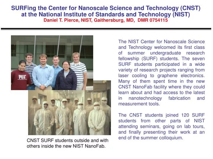
SURFing the Center for Nanoscale Science and Technology (CNST) at the National Institute of Standards and Technology (NIST)Daniel T. Pierce, NIST, Gaithersburg, MD, DMR 0754115 The NIST Center for Nanoscale Science and Technology welcomed its first class of summer undergraduate research fellowship (SURF) students. The seven SURF students participated in a wide variety of research projects ranging from laser cooling to graphene electronics. Many of them spent time in the new CNST NanoFab facility where they could learn about and had access to the latest in nanotechnology fabrication and measurement tools. The CNST students joined 120 SURF students from other parts of NIST attending seminars, going on lab tours, and finally presenting their work at an end of the summer colloquium. CNST SURF students outside and with others inside the new NIST NanoFab.
SURFing the Center for Nanoscale Science and Technology (CNST) at the National Institute of Standards and Technology (NIST)Daniel T. Pierce, NIST, Gaithersburg, MD,DMR 0754115 James MacArthur, a sophomore from Swarthmore College, implemented a lithography process based on laser interference to create regular arrays of long, straight magnetic stripes. The stripes are an ideal way to highlight and study the edge properties of patterned nanostructures. The magnetic properties of these stripes will be measured using newly developed microwave methods. To produce the nanostripes James had to master laser optics and clean room deposition procedures in the CNST NanoFab. His work has also caught the interest of other NanoFab users who need large, regular arrays of patterned structures as templates for directed self assembly. Intersecting beams of laser light (top) create an interference pattern (center) that exposes photoresist in a stripe pattern. A cross section of the developed resist (bottom) shows the ends of long parallel stripes. 200 nm wide NiFe stripes on Si