Download
1 / 15
150 likes | 349 Views
International Microwave Symposium 2011. A 3-Stage Shunt-Feedback Op-Amp having 19.2dB Gain, 54.1dBm OIP3 (2GHz), and 252 OIP3/P DC Ratio. Zach Griffith, M. Urteaga, R. Pierson, P. Rowell, M. Rodwell † , B. Brar Teledyne Scientific Company, Thousand Oaks, CA 91360, USA

E N D
International Microwave Symposium 2011 A 3-Stage Shunt-Feedback Op-Amp having 19.2dB Gain, 54.1dBm OIP3 (2GHz), and 252 OIP3/PDC Ratio Zach Griffith, M. Urteaga, R. Pierson, P. Rowell, M. Rodwell†, B. Brar Teledyne Scientific Company, Thousand Oaks, CA 91360, USA †Department of Electrical and Computer Engineering University of California, Santa Barbara, CA 93106-9560 e-mail: zgriffith@teledyne.com, phone: 805-373-4104
Standard design for low distortion amplification • In simple reactively-tuned RF amplifiers, the output-referred intermodulation distortion intercept (OIP3) is proportional to the DC current (i.e. DC power) dissipation • To have high OIP3 (very low power IM3 products), high bias currents and voltages are required • Continued system evolution (sensors, radar receivers, multi-carrier communications) requires increased linearity, dynamic range, and lower PDC • This is not possible with existing architectures, invariant of device bandwidth
linear response output power, dBm increasing feedback 2-tone intermodulation input power, dBm mm-wave Op-Amps for linear microwave amplification modern transistors have high bandwidth,can provide large feedback gain at 2-5 GHz. Strong negative feedback can greatly reduce distortion but: feedback helps less with stages near input and: any parasitic nonlinear feedback through transistor parasitics will ruin performance and: compensation for loop stability reduces feedback gain and increases distortion (slew rate) Nevertheless: ...with appropriate IC topologies ...and with fast devices100 GHz GBW op-amps and very low IM3 levels at 2-5 GHz
Strong global feedback strong linearization amplifiers with strong global negative feedback-- for linearization, gain control General form current summing voltage summing strong local negative feedback--- linearization weak shunt negative feedback--- for 50 Ohm Zin
Background: magnitude of local distortion generation The locally-generated distortion depends on the local signal level & the stage IP3 These locally-generated distortion signals are then suppressed ---in proportion to the amount of gain between that point and the input This is a simplified discussion, where a more complete analysis is included in the manuscript--- must consider voltages and currents,--- must consider frequency-dependent impedances
Challenges for low distortion, stable 50GHz op-amps • Technology: 0.5um InP HBT, 350GHz ft and fmax, ~5V breakdown • No InP HBT complimentary devices available • No active loads for high stage gain • RF choke inductor needed, effective at 2GHz Z = R + jL • Positive level-shifting not available • Bias currents and voltages carefully selected for low local-stage IM3 • Voltage difference across the feedback network must be considered • Non-linear capacitive loading of the HBT junction capacitances on the feedback network can introduce distortion that is not suppressed by strong feedback • Current summing avoids device Cje, Ccb loading of the feedback network • Amplifiers must be stable across its bandwidth for varying source impedance • Low noise figure – small input padding resistance Rin = 5-Ohm used • Feedback network must be electrically short at 50GHz • Low-power budget PDC ≤ 1.0W
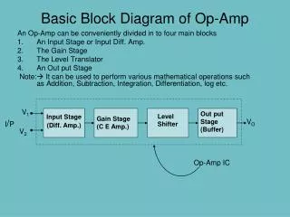
Differential current-mode building blocks Simple-Miller example – basic differential amplifier building blocks -- simple differential pair (gm,1gm,2) and Darlington differential pair amplification (gm,3) Simple differential pair, split current biasing Darlington differential pair used for the output stage
Differential Op-amp floorplan Simple-Miller schematic Detailed Simple-Miller floorplan Because the passives are large, all biasing components and loading elements are pulled away from the forward signal path and feedback network Only transistors and horizontal interconnects set the length of the feedback path
Equivalent half circuit – bias conditions HBT base-collector voltage is Vcb > 300mV to keep small distortion due to modulation of the capacitance Ccb Equivalent op-amp half-circuit Circuit floor plan Self-biasing voltages are set by previous stage current and load resistance
Layout and IC micrograph Circuit floorplan, Simple-Miller op-amp Dimensions: 0.92 x 0.46-mm2 Output, differential V2 V1 Input, differential Circuit layout IC micrograph of TSC fabricated op-amp Feedback path is short, only ~ 65m The electrical length of the feedback path is only… 3.5 degrees (/100) at 25GHz operation 14 degrees (/25) at 100GHz operation
Amplifier measurements Two-tone testbench, schematic • VNA measurements: • 4-port S-parameters, 100MHz-50GHz (Agilent PNA-X) • Discrete measurements of each port • Differential amplifier performance computed • True-mode differential stimulus to be performed • Two-tone and IM3 distortion measurements: • Agilent 4440A spectrum analyzer • Use of attenuators, isolators, and low-pass filters are required for very low VSWR throughout the system • Residual overall system distortion is 56dBm • From thru-lines probed on cal substrate Two-tone testbench, measurement Amplifier
Amplifier measurement: Differential S-parameters Differential S-parameters, measured Differential S-parameters, simulated Dashed line = as fabricated Solid line = additional AC ground strap • Inadequate interconnect at the emitter of the output stage differential pair causes excessive phase accumulation at higher frequency • This was not fully modeled during design • Re-evaluation by simulation shows the peaking observed in measurement • Additional emitter ground straps (w/ no other changes) greatly improves phase margin and the gain peaking is greatly reduced S21, mid-band = 19.2dB Bandwidth, 3dB > 30GHz Noise figure = 5.5dB PDC = 1020mW
Amplifier measurement: Two-tone power and IM3 Variation of OIP3 (2GHz) with Pout Pout, PIM3 versus Pin OIP3, 2GHz = 54.1dBm OIP3 to PDC ratio = 252 S-3BP at Pout = 16.6mW/tone OIP2 (f1+f2) > 90dBm Simulated OIP3 over frequency
Summary • Shunt-feedback amplifiers demonstrating high OIP3 have been presented • OIP3 = 54.1dBm at 2GHz, Slope-3 breakpoint Pout = 16.6mW/tone • 19.2dB S21 gain • 5.5dB noise figure • PDC = 1020mW • Record OIP3/PDC ratio = 252 • Future work requires examining… • Current source biasing to decrease common-mode gain • Improved layout for higher loop bandwidth, higher loop gain at low-GHz • Single DC source biasing, remove bias sequencing • Improve input and output VSWR • This work has been sponsored by the DARPA FLARE program • Dr. Sanjay Raman, Program Manager • Dr. Richard Eden, Program oversight