Download
1 / 49
540 likes | 1.16k Views
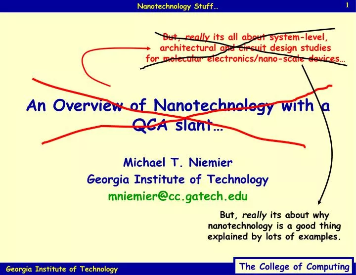
But, really its all about system-level, architectural and circuit design studies for molecular electronics/nano-scale devices… But, really its about why nanotechnology is a good thing explained by lots of examples. An Overview of Nanotechnology with a QCA slant… Michael T. Niemier

E N D
But, really its all about system-level, architectural and circuit design studies for molecular electronics/nano-scale devices… But, really its about why nanotechnology is a good thing explained by lots of examples. An Overview of Nanotechnology with a QCA slant… Michael T. Niemier Georgia Institute of Technology mniemier@cc.gatech.edu
Rocket Sun’s Nozzle Surface Nuclear Reactor CMOS IC 10000 Technical: 1000 Quantum effects,e- tunneling,power dissipation,slow wires, dopant concentrations,lithography resolutions, chip I/O,testing 100 Source: Borkar & De, Intel Power Density (W/cm2) Hot Plate 8086 10 P6 8008 Pentium® 8085 4004 386 286 486 8080 1 1970 1980 1990 2000 2010 Economical: 2010 fab plant may cost $200B! Technology paradigms 101 Past 7 decades, Zeus’s paradigm, current switches dominate: Vacuum tubes Solid-state transistors Electromechanical relay But problems lurk…
A cell with 4 dots Cell 2 Cell 2 Cell 1 Cell 1 • 2 extra electrons • Tunneling between dots An intro. to QCA • Conceptual Quantum-dot Cellular Automata (QCA) • Binary information encoded in charge configuration • QCA, CMOS, and Zuse’s paradigm: Cell-cell response function • Bi-stable, nonlinear cell-to-cell response • Restoration of signal levels • Robustness against Similar properties disorder cross implementation! Paradigm shift to molecular electronics QCA: molecules = charge containers, not current switches
Where do architects fit in? • CMOS provides faster devices, clocks, more computation • …but architects provide smartercomputation • Moore’s Law trends may be continued w/nano-scale devices • A particular focus: molecular nanoelectronics… • High functional density: 1011-1013 devices/cm2 (ideally 1014) • Ultimate limit of device scaling… • Most nano-scale devices targeted for computational systems • Architects understand them best • To complete the picture, we must answer: • Can we “compute” within different device paradigms? • Can system-level research help drive device research?
Other devices (& system studies) Device work: • Quantum transistors, RTDs, SETs, computing with molecules, CNT SiNW arrays, pure quantum computing, DNA-based computation, … Nano-tubes and Nano-wires: (Goldstein, Dehon) • Nanotube: nm wide metallic or semi-conducting tube • Applications… • Interconnect, SETs, micro- mechanical relays, levers… • Structures… • Arrays, crossbars, FPGAs, fabrics • “Compile to space, not time” • Challenges • Alignment, defects, interfacing, gain/signal restoration, customization Quantum computing: (Oskin, Chong, Chuang) • Only small devices (5-7 bits) built, lots of error correction, dataflow?
Early work:devices Device physics work… ey Custom work sets the stage for buildable designs ey q1 q2 = 0o 1 1 1 4 3 2 1 4 3 2 1 Progressed to simple Molecular device Design rules 3 3 3 3 circuits, architectures bridge the gap work 1 2 3 4 1 2 3 4 1 1 1 Algorithms to assist w/constraints mP, generic architectures 1 2 3 4 5 6 of QCA routing/layout next logical step Systems work… A B C D E F Roadmap
The Device P = +1 (Binary 1) P = -1 (Binary 0) Quantum Dot Electron A QCA Wire Signal Propagation Direction Majority Gate A 45-degree Wire Cell 2 (input) Input Cell (frozen polarization) Cell 4 (device) Original Propagation Direction 1 Cell 1 (input) Cell 5 (output) 2 Cell 3 (input) Complemented Copy But 1st…“Conceptual” QCA basics Wire Cross in the Plane 45-degree wire 90-degree wire (1st, basic Boolean logic, transistors)
Cells begin unpolarized • Barriers raised, • Barriers lowered • Cells relax to cells “latched” unpolarized state • Barriers held high • Used as input to next zone Release Relax • Barriers stay lowered • Cell remains in unpolarized/neutral state “Conceptual” QCA clock • CMOS clock: • controls memory transfers; 2 phases • QCA clock: • E-field controls barriers suppressing e- tunneling; 4 phases • QCA Clock phases: Switch Hold
And next, a conceptual clock structure “Schematic” Time Step 1 Switch Relax Release Hold Switch Time Step 2 Hold Switch Relax Release Hold Time Step 3 Release Hold Switch Relax Release Time Step 4 Relax Release Hold Switch Relax Time Step 5 Switch Relax Release Hold Switch Fixed Driver Wire Position A pipelined QCA wire. Each cell is clocked individually.
Electron (or a “hole” in this case) represents information + – – E “1” E-field – + + + “0” “null” E-field determines if cell active/null; driver determines 1 or 0 “0” “null” “1” “0” “null” mmolecule (eÅ) mMolecule (eA) mMolecule (eA) “1” mdriver (eÅ) clocking field (10-4 a.u.) Lent, Isaksen, Lieberman – Journal of the American Chemical Society mDriver (eA) mDriver (eA) An (implementable) clock structure
A QCA clock Silicon wires provide E-field A “top-down” view Input Cell (Conductor “up”) (Conductor “down”) Provides power gain and determinism in routing
QCA power dissipation For Reference… C • 2001 chip properties/info.: • On chip local clock frequencies B 1.77GHz, 122M transistors/chip • Chip dissipates 130W of power D • Average device power of A 1.07 mW/transistor, device (Courtesy of Craig Lent) switching energy of 0.6fJ • 2014 chip properties/info.: • On chip local clock frequencies 13.5GHz, 11,052M -- O(1010) transistors/chip • Chip dissipates 186W of power • Average device power of 16.8 nW/transistor, device switching energy of 1.25aJ J. Timler and C.S. Lent, J. Appl. Physics, Vol. 91 No. 2, 15 January 2002 • A, B: 2001 SIA Roadmap predictions for high-performance CMOS applications in 2001 and 2014 • C, D: Power delay properties of 30nm, 20nm gate transistors (2001 fabbed) QCA architectures can operate at densities above 1011 devices/cm2 without melting the chip.
Processor Control Memory Datapath Output Input Remember this slide? We’ll talk about stack, accumulator, and general purpose register machines in pictures particularly the datapath and memory components…
ALU What about this? (stack-based DF) Stack Pointer Memory PC IR Stack Top Address Why might we need all of these to form an address??? Flag Could do an operation with stack top and a value from memory… 1: Stack Top contains value 0: Stack Top is empty
MUX Memory A B ALU Acc Instruction Register Control Program Counter Or this? (Accumulator-based DF)
ALU Or this? (register based DF) OP i j k Register Write Memory Multi-port Register File Left Register Read Right Register Read $i $j op $k
A simple operation for each C = A + B (where A, B, and C are assumed memory addresses) Load/store assumes one can only access memory with load and store instructions Register/memory assumes one can access memory as part of any instruction. Could have 2 regs per inst. too…
New Mux B Mux B A We can lay this out in QCA cells. ALU PC/IR What the processor core can do: Can be built from functionally complete NAND logic • A + B • A AND B • B + 1 • 0 • A - B • A OR B • B Back to the accumulator-based DF. B-invert (AND/OR) Carry-in Zero A New mux Logic/Adder select Bmux select Accumulator Instruction Register Memory Read/Write Acc Read/write IR Memory write enable Select PC/IR as Program Counter memory address Read/write PC
Mead/Conway “Carrying a small design from conception through to… …completion provides the confidence [for] larger designs” Notre Dame Controlflow • No explicit flip-flop needed to store state Mux • State machine conventions change Acc Memory A B Instruction Register • Multiple state machines hard to ALU layout… Program Counter Dataflow Integration Control • Balancing routing and arrival • Power/density comparisons vs. CMOS of control/data signals very • Clock = inherent pipelining in data movement difficult in simplest of mPs • QCA circuits may be easily multi-threaded • Profitable to move logic into interconnect A custom mProcessor in QCA Overall: LAYOUT = TIMING!
1 2 3 4 Accumulator 1 1 Logic Unit 2 3 4 1 1 1 Output Mux 1 4 3 2 1 4 3 2 1 Adder Unit Intermediate ALU 3 3 3 3 signal generation logic Program Counter 1 2 3 4 1 2 3 4 1 1 1 B-Mux Floorplanning Why? Need clock for physical operation clock causes inherent pipelining… Shaded area = clocking zone in specific phase #s = relative clock phase Efficient/regular 2D wire routing Multiple wire loops, crossings, feedback Generalize to useful floorplans (i.e. foundations for real designs)
1 2 3 4 1 1 2 3 4 1 Affecting device development This floorplan functionality seen here… Device physicists/EEs studying how to build/implement/test/simulate our floorplan functionality Logic on top of wires Courtesy of Craig Lent (input) (device) (input) (output) (input)
Oh yeah…QCA potentially 400x denser than CMOS equivalent… Intermediate ALU signal generation logic Architectural innovations Accumulator Feedback trapezoid Zero A u Logic Unit Logic Logic u u u Unit These wires connect to form feedback path Output Mux “Processing-in-Wire” Adder • Data in feedback path pipelined back to start Program Counter • Do useful computation in feedback path Multithreading • The u’s represent potential threads B-Mux • Open ?s: # of threads, control logic
Acc Instruction Register Data from memory (for LOAD/arith. instruction) N Memory-to-IR IR-to-ALU G I Q New Mux PC-to-Bmux feedback Shows consequences (loads inst. into IR) (loads PC for JMP) Bmux select “pipelining provides”: F B Mux J Acc-to-ALU feedback Computation ballistic! Memory P A E Read/Write IR B Before: processing is A B Program Counter what’s possible in 1 Zero A ALU Logic/Adder Memory write time step enable B-invert (AND/OR) S D Carry-in R Now, coordinate Read/Write Read/Write H PC/IR ACC PC signal arrival times to C ensure processing will M K occur at all IR-to-memory path (for STORE instruction) Acc-to-memory feedback PC-to-memory path L Pipelining, latching, and theSimple 12 dataflow JMP ADD Select PC/IR as memory addr.
QCA controlflow A brief “case study” – control logic for Simple 12 Execute state bit/CZ Start A(11) A(10) Start A(11) Execute state A(10) Stopped state bit/CZ Stopped state Execute state bit/CZ iFetch state iFetch state bit/CZ • No need for explicit “flip-flops” – clocking zones latch data • Ideal design – all logic fits into 4 clocking zones and 1 “clock cycle” • 1 QCA clock when one clock zone cycles through 4 clock phases • But latching in each time step – analogous to “old” CMOS clock
Design Constraints • In the “near term”, we should target systems with: • Only 1 type of cell • (Hence no wire crossings) • Small systems • Systems that can be made up from many copies of the same component • Things that are simple, regular, replicable… (i.e. FPGA) • May not be most computationally interesting but… • Can get us to something computationally interesting and buildable • Helps physical scientists to design right device characteristics • Allows CS to explore requirements for more complex systems and architectures…
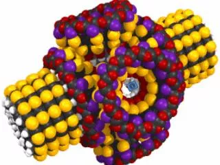
Non-lithographic patterningw/DNA tiles (“real” building blocks) • Double-crosslinked DNA tiles (Winfree, Lu, Wenzler, and Seeman, Nature 394, p. 539 (1998)) • Watson-Crick complement • Wang tiles
Genomic QCA circuit design • Program attachment points for QCA molecules • DNA tiles make printed circuit boards for QCA (Huber and Lent) Circuit design genome Circuit Circuit design information is impressed genetically rather than lithographically.
A problem with QCA: • No natural “switch” • Nearness needed for data movement Can we multiplex data? Interconnect area • Areas do not scale well Memory area • Quickly approach XILINX Logic area 4000 densities with much less functionality S2 S2 (Xilinx 4000) S1 S1 0 0 S0 S0 Determinism with the clock… SEL SEL • Clock selectively “turns off” QCA cells to S2 S2 create switches S1 S1 0 0 S0 S0 SEL SEL • “Lines” can be turned on or off • Pass transistors allow movement in multiple directions Transition to FPGAs… A “generic” FPGA: • Horizontal & vertical wires with programmable connections for data routing…
A B C Something more “implemetable” Lines = possible interconnection paths (deterministically controlled by clock) A 80 nm B C If NAND inputs are A, B, C, possible combinations are: 1. A NAND B 2. A NAND C 3. B NAND C 4. B NAND B Outstanding Issues: 120 nm • Design size must be scaled up because of limiting CMOS clock wire pitch • Logic block functionality can increase
** c ** c 99 9 ** 9 99 ** b 99 ** a 7 14 17 22 5 ** c 99 99 8 99 99 99 6 13 16 21 24 99 99 99 99 12 99 4 20 99 26 27 29 30 ** e 3 11 ** e 25 28 99 ** a 2 99 99 19 23 99 99 ** a 1 10 15 18 99 99 99 Simple 12 processor core 640 nm Serial input with delays 960 nm
Details and Issues QCA molecule DNA tile “Grid” of DNA CMOS wires underneath QCA • Etch out wire connections • Nanowires Connections to CMOS clock wire • Pass transistors • Vias CMOS clock wire
Architectural conclusions • QCA is envisioned as a deterministic processing device • If not easily obtainable via device fabrication… • …we can obtain with the clock • Determinism must come via fabrication or timing • Area comparisons: • Finally, area comparison comments still not exactly fair… • Logic block uses just a single NAND gate! • Inherent latching can eliminate need for physical registers
1 2 3 1 2 3 4 5 6 5 4 6 We can rearrange nodes to eliminate crosses Input A Input A y x Majority Gate Input B Input B Window of computation Input C Input C 0 (and) 1 (or) xor B A M M M A A xor B B B xor A 0 (and) A “logical” wire crossing XOR: (A and B’) or (A’ and B) (there is an inherent crossing) Using planar XOR made of NAND gates, circuit at left can be built CAD Buildability Constraints Rearrange to eliminate crosses Duplicate to eliminate crosses The building blocks that currently make up our “parts library” are restricted to the DNA-based substrates (Fig. 9a), circuits that use only 1 type of cell (i.e. only 90-degree cells), and circuits that have no wire crossings. A B B A B A B C D C D C D no crossing eliminated buildability constraints met by duplicating a node Logical crossings are also possible… Minimize clock skew Improve circuit density Because of QCA’s clock, only certain # of cells are active (able to compute) at any one time. If it takes too long for a value to propagate, the wrong answer will appear at the output. CAD can address this problem by optimizing for path length – or, as the clock moves from left to right, reducing the vertical height of wires (i.e. length x is shorter than length y). This is the first cut of an ALU; it is much less dense than equivalent designs.
w1 = 1 w2 = 0 w3 = 1 xin xin xin Systolic Architectures… Example Assume that we have a vector x = {1,1,0,1,0,1} and a vector w = {1,0,1} – we want to find all instances of 101 (the weights in the input vector 110101 (x). Note, that here all x’s would have to arrive simultaneously at each of the three blocks and thus would have to fan in as shown… xin initialize to 1 yi A B C We want to compute: yi = w1x1 + w2x2 + … + wkxi+k-1 This translates to: y1 = w1x1 + w2x2 + w3x3 y2 = w1x2 + w2x3 + w3x4 y3 = w1x3 + w2x4 + w3x5 y4 = w1x4 + w2x5 + w3x6 Pattern match Cycle 4: 1 1 0 1 0 1 1 0 1 Cycle 6: 1 1 0 1 0 1 1 0 1
Aout Cout Bout Ay By Cy w1=1 w2=0 w3=1 Ax Cx Bx xin A B C Systolic Architectures… It’s also possible to design a similar circuit without the requirement that all signals will have to arrive simultaneously. This circuit is shown below. This circuit will take longer to process the output. Also, x values will have to be asserted for two clock cycles as opposed to 1. Thus, an input pattern would be x1, x1, x2, x2, x3, x3, … Aout Ay Bout Cout Cy By Yout Yin based on… w3 = 1 w2 = 0 w1 = 1 W xin Ax Bx Xin Xout B C A
d c Systolic Processing (and errors) Sources of error a a b b …. c d e Possible sources of error in systems of molecular QCA cells. Missing cells (a), wrong distance between cells (b), offcenter cells (c), rotated cells (d), and offcenter cells in the “y”-dimension (e). The QCA circuit in terms of logic gates w2(0) w3(1) The top part of this figure shows a DNA tile with four schematic QCA molecules attached to specific sites in the major groove of one DNA helix (a). This DNA tile is one of nine tiles which would form a diamond-shaped raft 60 nm long by 12 nm wide. After ligation to prevent disassembly, six of these rafts would assemble (b) into a functional pattern matching circuit in an area of less than 0.01 square microns. Part (c) shows how the DNA circuit board could self-assemble on a surface with buried clocking wires; the wires are about 25 nm in diameter on a 75 nm pitch. This circuit would be capable of matching a specific string of 1s and 0s to an input stream of 1s and 0s – hardware that could be used in internet search engines to locate items in a database, to find an address in a computer’s memory, etc. xout xout xin xin
Not until thicker wires Must ensure no considered cross-talk b/t wires; also CMOS clock CMOS clock fields; QCA wire crossings, majority gates Comparison to CMOS Components of CMOS and QCA circuits CMOS QCA 90-degree 45-degree Permanent metal Diffusion cell cell cell contact Polysilicon substrates wells (i.e. DNA) substrates clock structures … & how they are analogous to QCA Types of CMOS design rules • Minimum width for current flow • Minimum spacing b/t entities • Required overlap to create devices • All allow for sources of error… • …ensure correct operation post-fab.
Example design rule Rule 2B: Disorder How is disorder affected by Ekink? 2B q Ekink ~ (1/r5)(cos4q) As qincreases, Ekink decreases. r ndisordered = # cells q1 q2 = 0o Ekink ~ (1/r5)(cos2(q 1+ q 2)) As q1 or q2increases, Ekink decreases. (also explains 45/90-degree interactions… Ekink = 0, therefore no interactions) ndisordered = # cells Why they are important: • Successful binary value transmission dependent on no external energy greater than the smallest kink energy
A few more design rules Rule 2C: Cross-talk 2C ey Minimum wire separation for no cross talk dmin Closest distance & still no cross talk dy Max error in placement y ey Why it is important: • dmin provides minimum separation between wires to ensure no cross-talk Rule 2D: A missing cell… 2D Cell missing: in part error defined by rule 1A Why it is important: • Helps to qualify error tolerances of wires
Other topics (without cool pictures yet) • Counterflow processor pipelines • Probabilistic Modeling • General purpose systolic processing • Non-QCA related material • May not be most computationally interesting but… • Can get us to something computationally interesting and buildable • Helps physical scientists to design right device characteristics • Allows CS to explore requirements for more complex systems and architectures…
“Big Picture” Conclusions • Find the determinism • If determinism cannot come from fabrication, we must find ways to do it with the clock • We need to create switches, E-field control important… • A “test bed” for QCA devices… • DNA, pass transistors not most optimal – but provides a test bed for QCA devices – performing computationally interesting tasks… • Nano #s are good… • 1st cut, NAND-based design is comparable with end of curve CMOS #s… • CS can affect PS… • Look toward an end goal (computational systems) • Identify what characteristics are essential and close the feedback loop…
Big Picture Conclusions (2) Next target for device physicists Theoretical Designs “Buildable” Designs Version 1… Version n… Version 10 Version 11 Architectural/circuit functionality
Cross-over Courtesy of Craig Lent
Double cross-over Courtesy of Craig Lent