Download
1 / 36
400 likes | 554 Views
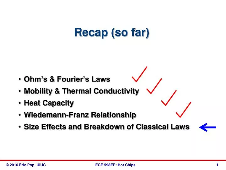
Recap (so far). Ohm’s & Fourier’s Laws Mobility & Thermal Conductivity Heat Capacity Wiedemann-Franz Relationship Size Effects and Breakdown of Classical Laws. Low-Dimensional & Boundary Effects. Energy Transport in Thin Films, Nanowires, Nanotubes Landauer Transport

E N D
Recap (so far) Ohm’s & Fourier’s Laws Mobility & Thermal Conductivity Heat Capacity Wiedemann-Franz Relationship Size Effects and Breakdown of Classical Laws
Low-Dimensional & Boundary Effects Energy Transport in Thin Films, Nanowires, Nanotubes Landauer Transport Quantum of Electrical and Thermal Conductance Electrical and Thermal Contacts Materials Thermometry Guest Lecture: Prof. David Cahill (MSE)
“Sub-Continuum” Energy Transport tsi Ox Si • Macroscale (D >> L) • Nanoscale (D < L) Me Ox D • Size and Non-Equilibrium Effects • optical-acoustic • small heat source • impurity scattering • boundary scattering • boundary resistance L ~ 200 nm Si
D ~ L D ~ l Thermal Simulation Hierarchy Continuum Fourier’s Law, FE MFP ~ 200 nm at 300 K in Si lattice wave D Phonon Transport BTE & Monte Carlo defect phonon Waves & Atoms Waves & Atoms MD & QMD Wavelength
Atomistic BTE with Wave models Sverdrup, Ju, Goodson (2000) BTE or Monte Carlo Phonons Lai, Majumdar (1995) much work Wachutka (1994) Diffusion Shur (1990) Apanovich (1995) Thermal and Electrical Simulation electrons phonons MFP ~5 nm ~100 nm l ~5 nm ~1 nm Bloetekjaer (1970) Baccarani (1985) Rudan (1986) Jacoboni (1983) Fischetti (1988) Lundstrom Datta (1995) Winstead (2003) Stratton (1962) Isothermal Drift Diffusion BTE Moments Monte Carlo & BTE Monte Carlo with Quantum Models Full Quantum Electrons
Nanowire Formation: “Bottom-Up” • Vapor-Liquid-Solid (VLS) growth • Need gas reactant as Si source (e.g. silane, SiH4) • Generated through • Chemical vapor deposition (CVD) • Laser ablation or MBE (solid target) Lu & Lieber, J. Phys. D (2006)
“Top-Down” and Templated Nanowires • “Top-down” = through conventional lithography • “Guided” growth = through porous templates (anodic Al2O3) • Vapor or electrochemical deposition Suspended nanowire (Tilke ‘03)
Semimetal-Semiconductor Transition • Bi (bismuth) has semimetal-semiconductor transition at wire D ~ 50 nm due to quantum confinement effects Source: M. Dresselhaus (MIT)
When to Worry About Confinement 2-D Phonons 2-D Electrons d d
Nanowire Applications • Transistors • Interconnects • Thermoelectrics • Heterostructures • Single-electron devices
Nanowire Thermal Conductivity Nanowire diameter Li, Appl. Phys. Lett. 83, 3187 (2003)
Interconnects = Top-Down Nanowires Intel 65 nm SEM of AMD’s “Hammer” microprocessor in 130 nm CMOS with 9 copper layers Cross-section 8 metal levels + ILD Transistor M1 pitch
Cu Resistivity Increase <100 nm Lines • Size Matters • Why? • Remember Matthiessen’s Rule
Cu Interconnect Delays Increase Too Source: ITRS http://www.itrs.net
Industry Acknowledged Challenges Source: ITRS http://www.itrs.net
Cu Resistivity and Line Width Steinhöglet al., Phys. Rev. B66 (2002)
Modeling Cu Line Resistivity Steinhöglet al., Phys. Rev. B66 (2002)
Model Applications Steinhöglet al., Phys. Rev. B66 (2002) Plombonet al., Appl. Phys. Lett 89 (2006)
Other Material Resistivity and MFP • Greater MFP (λ) means greater impact of “size effects” • Will Aluminum get a second chance?!
Same Effect for Thermal Conductivity! • Recall: • bulk Si kth ~ 150 W/m/K • bulk Ge kth ~ 60 W/m/K • Approximate bulk MFP’s: • λSi ~ 100 nm • λGe ~ 60 nm • Material with longer (bulk, phonon-limited) MFP λ suffers a stronger % decrease in conductivity in thin films or nanowires (when d ≤ λ) • Nanowire (NW) data by Li (2003), model Pop (2004) (at room temperature)
Back-of-Envelope Estimates (at room temperature)
More Sophisticated Analytic Models δ = d/λ< 1 S = (1 – δ2)1/2 Flik and Tien, J. Heat Transfer (1990) • Goodson, Annu. Rev. Mater. Sci. (1999)
A Few Other Scenarios anisotropy Goodson, Annu. Rev. Mater. Sci. (1999)
Onto Nanotubes… • Nanowires: • “Shrunk-down” 3D cylinders of a larger solid (large surface area to volume ratio) • Diameter d typically < {electron, phonon} bulk MFP Λ: surface roughness and grain boundary scattering important • Quantum confinement does not play a role unless d < {electron, phonon} wavelength λ ~ 1-5 nm (rarely!) • Nanotubes: • “Rolled-up” sheets of a 2D atomic plane • There is “no” volume, everything is a surface* • Diameter 1-3 nm (single-wall) comparable to wavelength λ so nanotubes do have 1D characteristics b * people usually define “thickness” b ~ 0.34 nm
Single-Wall Carbon Nanotubes • Carbon nanotube = rolled up graphene sheet • Great electrical properties • Semiconducting Transistors • Metallic Interconnects • Electrical Conductivity σ≈ 100 x σCu • Thermal Conductivity k ≈ kdiamond ≈ 5 x kCu d ~ 1-3 nm HfO2 CNT • Nanotube challenges: • Reproducible growth • Control of electrical and thermal properties • Going “from one to a billion” top gate (Al) S (Pd) D (Pd) SiO2
Fe Nanoparticle-Assisted Nanotube Growth • Particle size corresponds to nanotube diameter • Catalytic particles (“active end”) remain stuck to substrate • The other end is dome-closed • Base growth
Water-Assisted CVD and Breakdown • People can also grow “macroscopic” nanotube-based structures • Nanotubes break down at ~600 oC in O2, 1000 oC in N2 in O2 in N2 Hata et al., Science (2004)
Graphite Electronic Structure b ~ 3.4 Å acc~ 1.42 Å |a1|= |a2| = √3acc http://www.photon.t.u-tokyo.ac.jp/~maruyama/kataura/discussions.html
Nanotube Electronic Structure EG = 0 EG > 0 Collins and Avouris, Scientific American (2000) EG = 0 EG > 0
Band Gap Variation with Diameter • Red: metallic • Black: semiconducting Charlier, Rev. Mod. Phys. (2007) E11,M E22,M E22,S E11,M E11,S = EG ≈ 0.8/d “Kataura plot” http://www.photon.t.u-tokyo.ac.jp/~maruyama/kataura/kataura.html
Nanotube Current Density ~ 109 A/cm2 • Nanotubes are nearly ballistic conductors up to room temperature • Electron mean free path ~ 100-1000 nm CNT S (Pd) D (Pd) SiO2 L = 60 nm VDS = 1 mV G (Si) Javey et al., Phys. Rev. Lett. (2004)
Transport in Suspended Nanotubes E. Pop et al., Phys. Rev. Lett. 95, 155505 (2005) 2 μm nanotube on substrate suspended over trench nanotube Pt Pt gate Si3N4 SiO2 • Observation: significant current degradation and negative differential conductance at high bias in suspended tubes • Question: Why? Answer: Tube gets HOT (how?)
I2(R-Rc) TOP Non-equilibrium OP: ROP TAC = TL Heat transfer via AC: RTH T0 I2(R-RC) oxidation T TOP TAC = TL Optical TOP Acoustic TAC Transport Model Including Hot Phonons E. Pop et al., Phys. Rev. Lett. 95, 155505 (2005) Landauer electrical resistance Include OP absorption:
Extracting SWNT Thermal Conductivity E. Pop et al., Nano Letters 6, 96 (2006) • Ask the “inverse” question: Can I extract thermal properties from electrical data? • Numerical extraction of k from the high bias (V > 0.3 V) tail of I-V data • Compare to data from 100-300 K of UT Austin group (C. Yu, NL Sep’05) • Result: first “complete” picture of SWNT thermal conductivity from 100 – 800 K Yu et al. (NL’05) This work ~1/T ~T