Download
1 / 14
140 likes | 246 Views
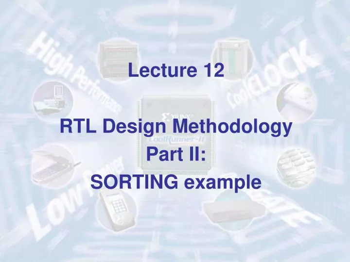
Lecture 12 RTL Design Methodology Part II: SORTING example. Structure of a Typical Digital System. Data Inputs. Control Inputs. Control Signals. Datapath ( Execution Unit ). Control ler (Control Unit ). Status Signals. Data Outputs. Control Outputs.

E N D
Lecture 12 RTL Design Methodology Part II: SORTING example
Structure of a Typical Digital System Data Inputs Control Inputs Control Signals Datapath (Execution Unit) Controller (Control Unit) Status Signals Data Outputs Control Outputs
Hardware Design with RTL VHDL Interface Pseudocode Datapath Controller Block diagram State diagram or ASM chart Block diagram VHDL code VHDL code VHDL code
Steps of the Design Process • Text description • Interface • Pseudocode • Block diagram of the Datapath • Interface divided into Datapath and Controller • ASM chart of the Controller • RTL VHDL code of the Datapath, Controller, and Top-Level Unit • Testbench for the Datapath, Controller, and Top-Level Unit • Functional simulation and debugging • Synthesis and post-synthesis simulation • Implementation and timing simulation • Experimental testing using FPGA board
Steps of the Design ProcessIntroduced in Class Today • Text description • Interface • Pseudocode • Block diagram of the Datapath • Interface divided into Datapath and Controller • ASM chart of the Controller • RTL VHDL code of the Datapath, Controller, and Top-level Unit • Testbench for theDatapath, Controller, and Top-Level Unit • Functional simulation and debugging • Synthesis and post-synthesis simulation • Implementation and timing simulation • Experimental testing using FPGA board
SORTING example
Sort Clock Resetn N N DataIn DataOut L RAdd Done WrInit S (0=initialization 1=computations) Rd Sorting - Required Interface
Simulation results for the sort operation (1)Loading memory and starting sorting
Simulation results for the sort operation (2)Completing sorting and reading out memory
Sorting - Example During Sorting After sorting Before sorting i=0 i=0 i=0 i=1 i=1 i=2 j=1 j=2 j=3 j=2 j=3 j=3 Address 0 1 2 3 3 3 2 2 1 1 1 1 2 2 3 3 3 3 2 2 4 4 4 4 4 4 4 3 1 1 1 1 2 2 3 4 Legend: position of memory indexed by i position of memory indexed by j Mj Mi
Pseudocode FOR k = 4 FOR any k ≥ 2 [load input data] wait for s=1 [load input data] wait for s=1 i = 0 2 for to do - i = 0 k 2 for to do Mi A = ; Mi A = ; j = i + 1 3 for to do – j = i + 1 k 1 for to do B = Mj ; B = Mj ; B < A if then B < A if then Mi = B ; Mi = B ; Mj = A ; Mj = A ; A = Mi ; A = Mi ; endif ; endif ; endfor; endfor; endfor; endfor; Done wait for s=0 [read output data] go to the beginning Done wait for s=0 [read output data] go to the beginning
Pseudocode wait for s=1 for i=0 to k-2 do A = Mi for j=i+1 to k-1 do B = Mj if A > B then Mi = B Mj = A A = Mi end if end for end for Done wait for s=0 go to the beginning
EN RST CLK DataIn RAdd 0 ABMux N L L N LD Li Resetn 1 0 s EN RST Ei CLK Din Clock s +1 Csel WrInit DIN We LD Lj WE 0 Resetn L Addr EN RST i Ej Wr ADDR 0 CLK Clock CLK 1 Clock L L j DOUT 1 N Mij = k-1 EB EA = k-2 Resetn Resetn EN RST CLK Clock Clock Rd zi N zj N N Bout 0 1 B A DataOut A>B Block diagram of the Datapath AgtB