Download
1 / 6
60 likes | 109 Views
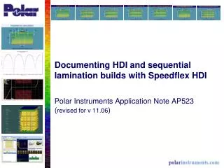
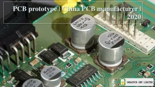
The function of such PCB is like at the electronic component level, this translates to components with increased I/Os with smaller footprint areas, and on the printed circuit board and package substrate level, to the use of high density interconnects (HDIs).

E N D
W WE EL LCO COME ME TO TO FPC CB.CO B.COM M E EFP W:www.efpcb.com S: shawnwang2006 E: sales@efpcb.com T: +86-755-23724206
Pcb Assembly, Pcba Immersion Gold Pcb,Gold Platting Pcb Lf Hasl Pcb Lead Free Hasl Pcb Backplane Board, Back Plane Pcb Impedance Control Pcb
Pcb Assembly,Printed Circuit Board Assembly Immersion Gold Pcb,94 V0 Pcb Micro Via Pcb, Multilayer Pcb High Temprature Pcb Metal Core Pcb, Aluminum Pcb, Led Pcb 0.2mm Thickness Fr4 Pcb
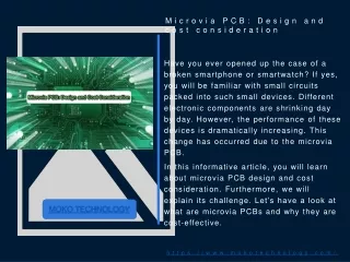
The concept of Microvias is very pervasive. These are used as the interconnects between layers in high density interconnect (HDI) substrates and printed circuit boards (PCBs) to accommodate the high input/output (I/O) density of advanced packages. Demand of HDI Microvia PCB is very high. Basing on the portability and wireless communications, the electronics industry strives to produce affordable, light, and reliable products with increased functionality. The function of such PCB is like at the electronic component level, this translates to components with increased I/Os with smaller footprint areas, and on the printed circuit board and package substrate level, to the use of high density interconnects (HDIs).
High Quality PCB Co., Limited Office address: Shajing Town,BaoanDistrict ,Shenzhen ,518000, China Plant 1 address: Building 5-6, Fu Qiao 3rd Industrial Zone, Bao' an, Shenzhen, Guangdong, China. Plant 2 address: Zhuhai, Guangdong,China Plant 3 address: Dongguan, Guangdong, China TEL: +86-755-23724206 Skype: shawnwang2006 Email: sales@efpcb.com http://efpcb.com/