1 / 8

Pin-Outs for Additional Hardware

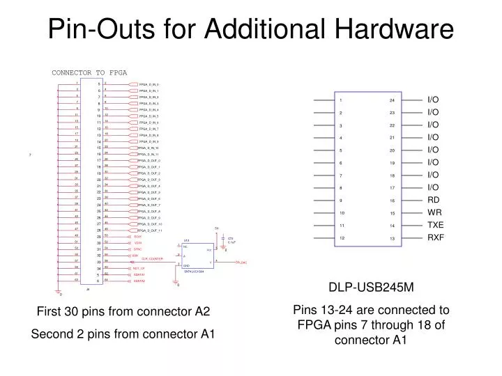
I/O. 1. 24. I/O. 23. 2. 5. I/O. 6. 22. 3. 7. I/O. 8. 21. 4. 9. I/O. 10. 5. 20. 11. I/O. 12. 6. 19. 13. I/O. 18. 14. 7. 15. I/O. 16. 8. 17. 17. RD. 9. 18. 16. 19. WR. 10. 15. 20. 21. TXE. 11. 22. 14. 23. RXF. 12. 13. 24. 25. 26. 27. 28. 29.

efia
Download Presentation

Pin-Outs for Additional Hardware

An Image/Link below is provided (as is) to download presentation Download Policy: Content on the Website is provided to you AS IS for your information and personal use and may not be sold / licensed / shared on other websites without getting consent from its author. Content is provided to you AS IS for your information and personal use only. Download presentation by click this link. While downloading, if for some reason you are not able to download a presentation, the publisher may have deleted the file from their server. During download, if you can't get a presentation, the file might be deleted by the publisher.

E N D

Presentation Transcript


  1. I/O 1 24 I/O 23 2 5 I/O 6 22 3 7 I/O 8 21 4 9 I/O 10 5 20 11 I/O 12 6 19 13 I/O 18 14 7 15 I/O 16 8 17 17 RD 9 18 16 19 WR 10 15 20 21 TXE 11 22 14 23 RXF 12 13 24 25 26 27 28 29 30 31 32 33 34 5 6 Pin-Outs for Additional Hardware 7 DLP-USB245M Pins 13-24 are connected to FPGA pins 7 through 18 of connector A1 First 30 pins from connector A2 Second 2 pins from connector A1

  2. Input Conditioning (Serial to Parallel Conversion)

  3. Output Conditioning (Parallel to Serial Conversion)

  4. Output Subsystem

  5. Input Subsystem

  6. Dual Buffer Layout

  7. USB Design Logic

  8. UART System

More Related